TWR-MCF5441X-KIT Freescale Semiconductor, TWR-MCF5441X-KIT Datasheet
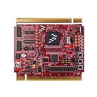
TWR-MCF5441X-KIT
Specifications of TWR-MCF5441X-KIT


Related parts for TWR-MCF5441X-KIT


TWR-MCF5441X-KIT Summary of contents
Page 1
... SHA-256 algorithms • Random number generator This document contains information on a new product. Specifications and information herein are subject to change without notice. © Freescale Semiconductor, Inc., 2010. All rights reserved. Preliminary—Subject to Change Without Notice MAPBGA–256 17mm x 17mm ® • ...
Page 2
... Rapid general purpose I/O timing specifications . . . . . 53 4.29 JTAG and boundary scan timing specifications . . . . . . 54 4.30 Debug AC timing specifications . . . . . . . . . . . . . . . . . . 56 5 Package information . . . . . . . . . . . . . . . . . . . . . . . . . . . . . . . 57 6 Product documentation . . . . . . . . . . . . . . . . . . . . . . . . . . . . . 57 7 Revision history . . . . . . . . . . . . . . . . . . . . . . . . . . . . . . . . . . . 58 ® Microprocessor Data Sheet, Rev. 6 Preliminary—Subject to Change Without Notice 2 C timing specifications . . . . . . . . . . . . . . . . . . . . . . . 45 Freescale Semiconductor ...
Page 3
... EMAC – Enchance multiply-accumulate unit EPORT – Edge port module GPIO – General purpose input/output module – Inter-Intergrated Circuit MCF5441x ColdFire Freescale Semiconductor MCF5441x BDM eDMA CAU Serial Boot RGPIO USB OTG Facility Crossbar Switch (XBS) Peripheral Bus Controller 1 1 Wire ...
Page 4
... Kbytes 8 Kbytes each — 2 ports 2 ports 2 ports channel 8 channel 8 channel Freescale Semiconductor ...
Page 5
... To further enhance noise isolation, an external filter is strongly recommended for the analog V VDDA_DAC_ADC). The filter shown in analog pins. The resistor and capacitors should be placed as close to the dedicated analog V in the given filter is required. MCF5441x ColdFire Freescale Semiconductor MCF54410 MCF54415 ...
Page 6
... GND Figure 2. ADC power filter 1 µF 0.1 µF GND Figure 3. IVDD power filter 1 µF 0.1 µF GND Figure 4. EVDD power filter ® Microprocessor Data Sheet, Rev. 6 Preliminary—Subject to Change Without Notice VDD_OSC_A_PLL VSS_OSC VDDA_ADC IVDD EVDD Freescale Semiconductor ...
Page 7
... EV DD All I/O VDD pins must be powered on when the device is functioning, except when in standby mode. In standby mode, all I/O VDD pins, except VSTBY_RTC (battery), can be switched off. MCF5441x ColdFire Freescale Semiconductor 1 µF GND Figure 5. FB_VDD power filter (EV ), FlexBus V ...
Page 8
... V during power down or there will be undesired high DD supplies VDD_OSC_A_PLL ® Microprocessor Data Sheet, Rev. 6 Preliminary—Subject to Change Without Notice , FBV , or SDV FBV , or SDV must power down Symbol Typical Unit IVDD 127 9.3 9.2 3.6 3.4 FBVDD SDVDD SDVREF 1.3 SDVTT Freescale Semiconductor by more DD DD ...
Page 9
... The primary functionality of a pin is not necessarily its default functionality. Most pins that are muxed with GPIO default to their GPIO functionality. See exceptions. MCF5441x ColdFire Freescale Semiconductor VDDA_DAC_ADC NOTE NOTE ® Microprocessor Data Sheet, Rev. 6 Preliminary— ...
Page 10
... I EVDD ae G14 — O EVDD ae H14 — I EVDD msr G5,H5 — I/O FBVDD fsr A10, A9, B9, C9, A8, B8, C8, A7 — I/O FBVDD fsr B7, C7, C6, B6, A6, A5, B5, A4 Freescale Semiconductor K15 L16 G16 H16 K5, L5 B9, C8, A9, B8, D8, A8, D7, B7 C7, A7, D6, A6, B6, D5, C6, A5 ...
Page 11
... FB_CS5 PB6 FB_CS4 PB5 FB_CS1 PB4 FB_CS0 PB3 I2C0_SCL PB2 I2C0_SDA PB1 CAN1_TX PB0 CAN1_RX PC7 SD_A14 — MCF5441x ColdFire Freescale Semiconductor Alternate 1 Alternate 2 — — — — — — FB_TS — FB_TBST/ — NFC_RE — — — NFC_R/B FB_CS3 FB_A1/ ...
Page 12
... L7 — I EVDD ssr F12 — I EVDD — ssr — I EVDD ssr E11 — — I EVDD ssr 13 — — I EVDD ssr Freescale Semiconductor R4, R1, R3, N4, P3, T4, R2, T2, N3, P5, P4, N5, P2, T3 P7, N6 T12, R11, T11, R10, N9, T10, P9 P10 N10 F12 N1 F14 M1 M2 ...
Page 13
... RTC_XTAL — DSPI0_PCS1/ PC0 SBF_CS DSPI0_PCS0/SS PD7 DSPI0_SCK/ PD6 SBF_CK DSPI0_SIN/ PD5 SBF_DI DSPI0_SOUT/ PD4 SBF_DO MCF5441x ColdFire Freescale Semiconductor Alternate 1 Alternate 2 — — USB On-the-Go — — — — USB host — — — — ADC — — — ...
Page 14
... EVDD msr — I/O — EVDD msr — I/O — EVDD msr — I/O — EVDD msr — O — EVDD msr Freescale Semiconductor N11 G13 H14 H13 H15 C10 D10 C9 D9 E13 B11 B10 D11 B13 E14 D12 B12 C11 ...
Page 15
... MII0_CRS PK6 MII0_RXD[3:2] PK[5:4] MII0_RXCLK PK3 MII0_TXD[3:2] PK[2:1] MII0_TXCLK PK0 22 ALLPST PH2 DDATA[3:2] PH[1:0] DDATA[1:0] PI[7:6] MCF5441x ColdFire Freescale Semiconductor Alternate 1 Alternate 2 Smart card interface 0 PWM_FAULT2 SDHC_DAT7 PWM_FAULT0 — PWM_FORCE SDHC_DAT6 PWM_SYNC SDHC_DAT5 PWM_FAULT1 SDHC_DAT4 Synchronous serial interface 0 I2C2_SDA SIM1_VEN I2C2_SCL ...
Page 16
... F11 — — — vdde — — — — — — — — — — vssint Freescale Semiconductor J13, J16, J15, J14 N15 M16 L13 K14 K16 K13 R16 E9–E11, F9–F11 K6–K11, L6 E5–E7, F5, F6, G5 M7–M12 F15 F16 ...
Page 17
... UARTx_TXD pad can act as RXD(input) pad when UART One Wire mode is enabled. 20 These RMII functions are selected by the mode chosen by the MAC-NET, not by the pin-multiplexing and control (GPIO) module. 21 Configurable pull that is enabled and pulled down after reset. MCF5441x ColdFire Freescale Semiconductor Alternate 1 Alternate 2 — — — ...
Page 18
... TDI TDO RSTOUT OW_ RMII0_ RMII0_ SD_D6 DAT RXER CRS_DV RMII0_ RMII0_ RMII0_ SD_D5 F TXD0 TXEN RXD0 RMII0_ RMII0_ SD_D3 SD_D7 TXD1 RXD1 Freescale Semiconductor 14 VSS A RTC_ B EXTAL RTC_ C XTAL VSS D VSTBY_ E RTC VSS_ OSC_A F _PLL EXTAL G XTAL H VSS J RESET K TCLK L ...
Page 19
... SD_A3 SD_A4 SD_A14 SD_BA2 RXD R SD_A12 SD_A7 SD_A11 SD_A13 SD_BA0 SD_ T VSS SD_A6 SD_A0 SD_A8 CLK Figure 8. MCF54415, MCF54416, MCF54417, and MCF54418 Pinout (256 MAPBGA) MCF5441x ColdFire Freescale Semiconductor FB_ FB_ FB_ FB_ SDHC_ AD20 AD22 AD26 AD29 CLK FB_ FB_ ...
Page 20
... VDD_USBO VDD_USBH –0.3 to +4.0 VDDA_ADC –0.3 to +4.0 VDDA_DAC_ADC –0.3 to +4.0 VSTBY_RTC –0.3 to +4.0 — –0.3 to +3.6 — 25 — –40 to +85 — –55 to +150 . DD , and SDV range during instantaneous and DD > FBV , or SDV ) is greater than Freescale Semiconductor Units C C ...
Page 21
... Solving equations 1 and 2 for K gives: where constant pertaining to the particular part. K can be determined from for a known T . Using this value of K, the values for any value MCF5441x ColdFire Freescale Semiconductor Table 7. Thermal characteristics Symbol 1,2 Four layer board JA (2s2p) 1,2 ...
Page 22
... Preliminary—Subject to Change Without Notice 1, 2 Value Units 2000 V Conditions II level A II level Min Max IVDD 1.14 1.32 1.71 3.63 1.71 1.98 0.49 x SDV 0.51 x SDV DD SDV – 0.04 SDV + 0.04 REF REF 3.135 3.63 A_PLL EVDD 3.135 3.63 Freescale Semiconductor Class Units ...
Page 23
... OH FlexBus output low voltage @ 1.8V–3. 5.0 mA for all modes OL Input Leakage Current Input-only pins Weak internal pull-up/pull-down device current MCF5441x ColdFire Freescale Semiconductor Symbol Pin Name USBV VDD_USBO DD VDD_USBH AV VDDA_ADC DD — VDDA_DAC_ RTCV VSTBY_RTC STBY Table 11. I/O electrical specifications Symbol ...
Page 24
... Microprocessor Data Sheet, Rev. 6 Preliminary—Subject to Change Without Notice Min Max Units A 25 150 pF — 7 — 200 lists the rise/fall time for pins based on the Rise/fall time (ns) 2 210 220 Freescale Semiconductor ...
Page 25
... For a single device drive, this setting should enable Full Strength mode. High Strength is intended for multiple device drives (DIMM). Pad type st MCF5441x ColdFire Freescale Semiconductor Table 12. Output pad slew rates (continued) Slew rate select Drive load field value (pF) ...
Page 26
... From crystal L spec R 10 — 200 S 2 C — – L_XTAL L C – S_XTAL 7 C PCB_XTAL 2 C — – – S_EXTAL 7 C PCB_EXTAL C jitter — 10 — 0.1 Freescale Semiconductor Unit MHz MHz MHz MHz MHz MHz M sys sys/3 . sys ...
Page 27
... RESET and configuration override data lines are synchronized internally. Setup and hold times must be met only if recognition on a particular clock is required. 2 During low power STOP, the synchronizers for the RESET input are bypassed and RESET is asserted asynchronously to the system. Thus, RESET must be held a minimum of 100 ns. MCF5441x ColdFire Freescale Semiconductor XOSC EXTAL R F Crystal or Resonator ...
Page 28
... EMI. MCF5441x ColdFire Table 16. FlexBus timing specifications Characteristic ® Microprocessor Data Sheet, Rev. 6 Preliminary—Subject to Change Without Notice Min Max Unit Notes — 62.5 MHz 16 — — 6 0.5 — 5.5 — — ns Freescale Semiconductor R8 ...
Page 29
... Note: 1 FB2 and FB3 output specifications are valid for all FB_AD[31:0], FB_R/W, FB_ALE, FB_TS, FB_CSn, FB_OE, FB_BE/BWEn, and FB_TSIZ[1:0]. 2 FB4 and FB5 input specifications are valid for all FB_AD[31:0] and FB_TA. MCF5441x ColdFire Freescale Semiconductor S0 S1 FB_CLK FB1 ADDR[Y:0] FB2 ADDR[31:X] ...
Page 30
... CLS t CLH ® Microprocessor Data Sheet, Rev. 6 Preliminary—Subject to Change Without Notice S2 S3 FB3 FB5 Min Max Unit 1 — 40 MHz 25 — ns 1.5 t — ns NFC t — ns NFC 1.5 t — ns NFC t — ns NFC 0.5 t – 0.5 — ns NFC Freescale Semiconductor ...
Page 31
... NF14 NFC_RE pulse width NF15 Read cycle time NF16 NFC_RE high hold time NF17 Data in setup time 1 50 MHz maximum frequency can only be used if the part is in EDO (enhanced data out) mode. NFC_CLE NFC_CE NFC_WE NFC_ALE NFC_IO[7:0] MCF5441x ColdFire Freescale Semiconductor Symbol t ALS t ALH ...
Page 32
... NF11 NF6 NF12 NF7 NF8 NF9 Address Figure 14. Address latch cycle timing NF11 NF6 NF12 NF7 NF9 Data to NF Figure 15. Write data latch timing ® Microprocessor Data Sheet, Rev. 6 Preliminary—Subject to Change Without Notice NF5 NF10 NF3 NF5 NF10 Freescale Semiconductor ...
Page 33
... The SDRAM interface operates at the same frequency as the internal system bus. 2 Pulse width high plus pulse width low cannot exceed min and max clock period. 3 Command output valid should be 1/2 the memory bus clock (t and voltage variations. MCF5441x ColdFire Freescale Semiconductor NF15 NF14 NF16 NF17 Data from NF NF13 Figure 16 ...
Page 34
... SD_RAS, SD_CAS DD4 SD_A[13:0] SD_DM SD_DQS SD_D[7:0] MCF5441x ColdFire 34 DD1 DD5 CMD DD6 ROW COL Figure 17. DDR write timing ® Microprocessor Data Sheet, Rev. 6 Preliminary—Subject to Change Without Notice DD2 DD3 DD7 DD8 DD7 WD1 WD2 WD3 WD4 DD8 Freescale Semiconductor ...
Page 35
... USB_CLKIN pin on the MCF5441x. The ULPI PHY is the source of the 60MHz clock. The USB controller requires a 60-MHz clock, even if using the on-chip FS/LS transceiver instead of the ULPI interface. In this case, the 60-MHz clock can be generated by the PLL or input on the USB_CLKIN pin. MCF5441x ColdFire Freescale Semiconductor DD1 DD5 CL=2 CMD ...
Page 36
... Table 19. ULPI interface timing Min — — — 5.0 1.0 — 1 Figure 19. ULPI timing diagram ® Microprocessor Data Sheet, Rev. 6 Preliminary—Subject to Change Without Notice Nominal Max Units 60 — MHz 50 — % 16.67 — ns — — ns — — ns — 9.5 ns — — Freescale Semiconductor ...
Page 37
... In card identification mode, card clock must be 100 kHz– 400 kHz, voltage ranges from 2.7 to 3.6 V. SDHC_CLK Output from eSDHC to card SDHC_CMD SDHC_DAT[3:0] Input from card to eSDHC SDHC_CMD SDHC_DAT[3:0] MCF5441x ColdFire Freescale Semiconductor Table 20 lists the eSDHC timing characteristics. Symbols SD2 SD4 SD5 SD3 SD6 SD7 Figure 20 ...
Page 38
... DD 0. 0.125 x V 0.625 – 0.3 0. ® Microprocessor Data Sheet, Rev. 6 Preliminary—Subject to Change Without Notice Unit Condition/remark k Internal PU NA k For MMC cards only For MMC cards only I = –100 µ 0 –100 µ 100 µ Freescale Semiconductor min DD min DD ...
Page 39
... The card must send a response on RX acknowledging the reset between 400 and 40,000 clock cycles after T0. SIM_VEN SIM_CLK SIM_RX Figure 22. Internal-reset card reset sequence MCF5441x ColdFire Freescale Semiconductor Table 22 lists the timing parameters. 1/Sfreq Sfall Srise Figure 21. SIM clock timing diagram Symbol 1 ...
Page 40
... MCF5441x ColdFire 40 Figure 23 400 clock cycles < 400,000 clock cycles < Figure 24 and Table 23 ® Microprocessor Data Sheet, Rev. 6 Preliminary—Subject to Change Without Notice Response 2 3 < 200 clock cycles 1 < 40,000 clock cycles 2 3 show the usual timing requirements for this Freescale Semiconductor ...
Page 41
... When operating this interface at lower frequencies, increase the slew rate by using the 10, 01 setting to increase edge rise and fall times, thus reducing EMI. MCF5441x ColdFire Freescale Semiconductor Symbol S rst2clk ...
Page 42
... Preliminary—Subject to Change Without Notice 1 Min Max Units Notes 2 15.15 — ns 45% 55% t MCLK 3 80 — ns 45% 55% t BCLK — — ns — — — — sys ). sys 1 Min Max Units Notes 80 — ns 45% 55% t BCLK 10 — — ns — — — — ns Freescale Semiconductor ...
Page 43
... SSI_FS (Input) S15 SSI_TXD SSI_RXD 4.18 12-bit ADC specifications Characteristic Frequency of operation ADC clock period Low reference voltage High reference voltage Integral non-linearity (10% to 90% input signal range) MCF5441x ColdFire Freescale Semiconductor S10 Figure 25. SSI timing — master modes S11 S12 S12 ...
Page 44
... Typical Max 806 — Guaranteed 1 — — 2 — — — 1M — — 500K — AVDD – 0.04 Freescale Semiconductor Unit lsb t cycles ADC t cycles ADC 5 t cycles ADC t cycles ADC LSB LSB % Bits Unit ...
Page 45
... I2C_SCL/I2C_SDA fall time (V I6 Clock high time I7 Data setup time I8 Start condition setup time (for repeated start condition only) I9 Stop condition setup time Table 30 lists specifications for the I MCF5441x ColdFire Freescale Semiconductor 1 Table 27. DAC parameters (continued) Name INL DNL E GAIN ENOB t DAPU ...
Page 46
... Microprocessor Data Sheet, Rev. 6 Preliminary—Subject to Change Without Notice Min Max Units 6 — 1/f SYS 10 — 1/f SYS — — µs 7 — 1/f SYS — — 1/f SYS 2 — 1/f SYS 20 — 1/f SYS 10 — 1/f SYS 2 Table 30. The I C interface Freescale Semiconductor ...
Page 47
... TXCLK frequency E5 TXCLK to TXD[n:0], TXEN, TXER invalid E6 TXCLK to TXD[n:0], TXEN, TXER valid E7 TXCLK pulse width high E8 TXCLK pulse width low 1 In MII mode RMII mode MCF5441x ColdFire Freescale Semiconductor Table 31. Receive signal timing MII mode Min Max — — — ...
Page 48
... Table 33. MII/RMII transmit signal timing Characteristic E9 Symbol t ® Microprocessor Data Sheet, Rev. 6 Preliminary—Subject to Change Without Notice E7 E5 Valid Data Min Max Unit 1.5 — TXCLK period Min Max Unit 400 — ns MDC MDC — 375 ns 25 — — — ns Freescale Semiconductor ...
Page 49
... When operating this interface at lower frequencies, increase the slew rate by using the 10, 01 setting to increase edge rise and fall times, thus reducing EMI. MCF5441x ColdFire Freescale Semiconductor E10 E11 E11 ...
Page 50
... Microprocessor Data Sheet, Rev. 6 Preliminary—Subject to Change Without Notice 1 (continued) Min Max Unit –5 — — — ns 8 — f MHz SYS 8 f — ns SYS 2) – 2.0 sck — — — — ns — — Freescale Semiconductor Notes ...
Page 51
... DSPI_SOUT Figure 32. DSPI Classic SPI timing — master Mode DSPI_SS DSPI_SCK (DCTARn[CPOL DSPI_SCK (DCTARn[CPOL DSPI_SOUT DSPI_SIN Figure 33. DSPI Classic SPI timing — slave mode MCF5441x ColdFire Freescale Semiconductor DS3 DS2 DS2 DS7 DS8 First Data Data DS5 First Data Data DS10 ...
Page 52
... Microprocessor Data Sheet, Rev. 6 Preliminary—Subject to Change Without Notice Min Max Unit — 62.5 MHz 16.67 — ns 30% — t SBFCK – 2.0 — ns – 2.0 — ns — –5 — — — ns SB4 Last Data SB6 Last Data Freescale Semiconductor Notes 1 ...
Page 53
... Num RG1 PST_CLK high to RGPIO output valid RG2 PST_CLK high to RGPIO output Invalid RG3 RGPIO input valid to PST_CLK high RG4 PST_CLK high to RGPIO input invalid MCF5441x ColdFire Freescale Semiconductor Table 38. GPIO timing Characteristic Figure 35. GPIO timing Table 39. RGPIO timing Characteristic ® ...
Page 54
... Figure 36. RGPIO timing 1 Table 40. JTAG and boundary scan timing 1 Characteristics ® Microprocessor Data Sheet, Rev. 6 Preliminary—Subject to Change Without Notice RG2 Min Max Unit DC 25 MHz 40 — — ns — — — ns — — — — ns — — — — ns Freescale Semiconductor ...
Page 55
... V IL Data Inputs Data Outputs Data Outputs Data Outputs TCLK V IL TDI TMS TDO TDO TDO TCLK TRST MCF5441x ColdFire Freescale Semiconductor Figure 37. Test clock input timing J5 Input Data Valid Figure 38. Boundary scan (JTAG) timing J9 Input Data Valid J11 J12 J11 Figure 39 ...
Page 56
... Figure 42. BDM serial port AC timing ® Microprocessor Data Sheet, Rev. 6 Preliminary—Subject to Change Without Notice Figure 41 and Table 42. Min Max Units 0.5 0.5 1/f SYS — 3.0 ns 0.5 — — PSTCLK 4 — PSTCLK 5 — PSTCLK 1 — PSTCLK D2 Next Current Freescale Semiconductor ...
Page 57
... MCF54418 6 Product documentation Documentation is available from a local Freescale distributor, a Freescale sales office, the Freescale Literature Distribution Center, or through the Freescale world-wide web address at http://www.freescale.com/coldfire. MCF5441x ColdFire Freescale Semiconductor Table 42. Package information Package type Case outline numbers 196 MAPBGA 98ARH98217A 256 MAPBGA 98ARH98219A ® ...
Page 58
... Microprocessor Data Sheet, Rev. 6 Preliminary—Subject to Change Without Notice MAPBGA” and updated SDCK Freescale Semiconductor Table 5 with ...
Page 59
... Added case outline numbers to Changed PLL supply voltage from “–0.5 to +2.0” to “–0.3 to +4.0” in Miscellaneous corrections based on information from shared review comments by team members MCF5441x ColdFire Freescale Semiconductor Table 43. Revision history (continued) Summary of changes Section 4.6, “Output pad loading and slew ...
Page 60
... Freescale Semiconductor product could create a situation where personal injury or death may occur. Should Buyer ...