13192DSK-A0E Freescale Semiconductor, 13192DSK-A0E Datasheet - Page 14
13192DSK-A0E
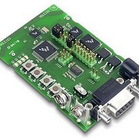
Manufacturer Part Number
13192DSK-A0E
Description
KIT DEV STARTER FOR 13191/92
Manufacturer
Freescale Semiconductor
Type
802.15.4/Zigbeer
Specifications of 13192DSK-A0E
Contents
Hardware, Software and Documentation
Wireless Frequency
2.4 GHz
Interface Type
SPI
Modulation
DSSS OQPSK
Security
128 bit AES
Silicon Manufacturer
Freescale
Silicon Core Number
MC13191, MC13192
Kit Application Type
Communication & Networking
Application Sub Type
Wireless Network
Kit Contents
13192 Developer Starter Kit
Rohs Compliant
Yes
For Use With/related Products
MC13191, MC13192
Lead Free Status / RoHS Status
Lead free / RoHS Compliant


Pin Connections
7
14
Pin #
10
12
13
14
15
16
17
18
19
11
1
2
3
4
5
6
7
8
9
Pin Connections
RFIN-
RFIN+
Not Used
Not Used
PAO+
PAO-
SM
GPIO4
GPIO3
GPIO2
GPIO1
RST
RXTXEN
ATTN
CLKO
SPICLK
MOSI
MISO
CE
Pin Name
2
2
2
3
1
1
1
1
2
2
RF Input
RF Input
RF Output /DC Input
RF Output/DC Input
Digital Input/ Output
Digital Input/ Output
Digital Input/ Output
Digital Input/ Output
Digital Input
Digital Input
Digital Input
Digital Output
Digital Clock Input
Digital Input
Digital Output
Digital Input
Type
Table 8. Pin Function Description
MC13192 Technical Data, Rev. 3.3
LNA negative differential input.
LNA positive differential input.
Tie to Ground.
Tie to Ground.
Power Amplifier Positive Output. Open drain. Connect
to V
Power Amplifier Negative Output. Open drain.
Connect to V
Test mode pin. Tie to Ground
General Purpose Input/Output 4.
General Purpose Input/Output 3.
General Purpose Input/Output 2. When gpio_alt_en,
Register 9, Bit 7 = 1, GPIO2 functions as a “CRC
Valid” indicator.
General Purpose Input/Output 1. When gpio_alt_en,
Register 9, Bit 7 = 1, GPIO1 functions as an “Out of
Idle” indicator.
Active Low Reset. While held low, the IC is in Off Mode
and all internal information is lost from RAM and SPI
registers. When high, IC goes to IDLE Mode, with SPI
in default state.
Active High. Low to high transition initiates RX or TX
sequence depending on SPI setting. Should be taken
high after SPI programming to start RX or TX
sequence and should be held high through the
sequence. After sequence is complete, return
RXTXEN to low. When held low, forces Idle Mode.
Active Low Attention. Transitions IC from either
Hibernate or Doze Modes to Idle.
Clock output to host MCU. Programmable frequencies
of:
16 MHz, 8 MHz, 4 MHz, 2 MHz, 1 MHz, 62.5 kHz,
32.786+ kHz (default),
and 16.393+ kHz.
External clock input for the SPI interface.
Master Out/Slave In. Dedicated SPI data input.
Master In/Slave Out. Dedicated SPI data output.
Active Low Chip Enable. Enables SPI transfers.
DDA
.
DDA
.
Description
Freescale Semiconductor
Tie to Ground for
normal operation
See Footnote 1
See Footnote 1
See Footnote 1
See Footnote 1
See Footnote 2
See Footnote 2
See Footnote 2
See Footnote 2
See Footnote 3
See Footnote 2
Functionality
Related parts for 13192DSK-A0E
Image
Part Number
Description
Manufacturer
Datasheet
Request
R

Part Number:
Description:
KIT DEV STARTERS FOR MC13191,192
Manufacturer:
Freescale Semiconductor
Datasheet:
Part Number:
Description:
KIT STARTER MC13191/92 W/CABLE
Manufacturer:
Freescale Semiconductor
Datasheet:
Part Number:
Description:
KIT DEV STARTER
Manufacturer:
Freescale Semiconductor
Datasheet:

Part Number:
Description:
Manufacturer:
Freescale Semiconductor, Inc
Datasheet:
Part Number:
Description:
Manufacturer:
Freescale Semiconductor, Inc
Datasheet:
Part Number:
Description:
Manufacturer:
Freescale Semiconductor, Inc
Datasheet:
Part Number:
Description:
Manufacturer:
Freescale Semiconductor, Inc
Datasheet:
Part Number:
Description:
Manufacturer:
Freescale Semiconductor, Inc
Datasheet:
Part Number:
Description:
Manufacturer:
Freescale Semiconductor, Inc
Datasheet:
Part Number:
Description:
Manufacturer:
Freescale Semiconductor, Inc
Datasheet:
Part Number:
Description:
Manufacturer:
Freescale Semiconductor, Inc
Datasheet:
Part Number:
Description:
Manufacturer:
Freescale Semiconductor, Inc
Datasheet:
Part Number:
Description:
Manufacturer:
Freescale Semiconductor, Inc
Datasheet:
Part Number:
Description:
Manufacturer:
Freescale Semiconductor, Inc
Datasheet:
Part Number:
Description:
Manufacturer:
Freescale Semiconductor, Inc
Datasheet: