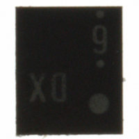
AN26210A-PB Panasonic - SSG, AN26210A-PB Datasheet - Page 6

AN26210A-PB
Manufacturer Part Number
AN26210A-PB
Description
IC LNA DUAL BAND W-CDMA
Manufacturer
Panasonic - SSG
Datasheet
1.AN26210A-PB.pdf
(26 pages)
Specifications of AN26210A-PB
Current - Supply
4.5mA
Frequency
800MHz, 2GHz
Gain
17dB
Noise Figure
1.55dB
P1db
-12dBm
Package / Case
12-XLGA
Rf Type
Cellular, GPS, W-CDMA
Test Frequency
2.1GHz
Voltage - Supply
2.7V ~ 2.95V
Lead Free Status / RoHS Status
Lead free / RoHS Compliant
Other names
AN26210A
AN26210A-PBTR
AN26210ATR
AN26210ATR
AN26210A-PBTR
AN26210ATR
AN26210ATR
Notes) Do not apply voltage to N.C. pins.
注) *1 : RF signal input pin. Do not apply DC current.
232621000606082
2007-02-27
Established
Pin No.
Current and Voltage Range for Pins
FIN1
FIN2
*2 : RF signal output pin. Do not apply DC current.
*3 : Same as GND pin
10
11
12
1
2
3
4
5
6
7
8
9
The values shows voltage to the GND unless otherwise specified. (+) is inlet current and (–) is outlet current in the circuit.
Voltage applying exceeding below ratings leads to the malfunction and the damage of the device.
Below ratings are specified regarding malfunction and stress, not for operation guaranty.
Pin name
GND3
CNT2
CNT1
OUT1
OUT2
GND
GND
GND
GND
IN2
IN1
Vcc
Vcc
E
Revised
– 0.3 to (V
– 0.3 to (V
– 0.3 to (V
– 0.3 to (V
– 0.3 to (V
0 to 3.0
0 to 3.0
Rating
—
—
0
0
0
0
0
CC
– 1 / 2)
CC
CC
CC
CC
Product Standards
)
)
)
)
Unit
V
V
V
V
V
V
V
V
V
V
V
V
V
V
Semiconductor Company, Matsushita Electric Industrial Co., Ltd.
Notes
*1
*3
*3
*1
*2
*2
Total Pages
26
AN26210A
Page
6


