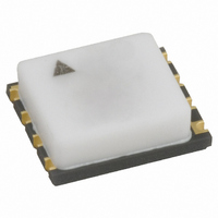
RF3800TR7 RFMD, RF3800TR7 Datasheet - Page 12

RF3800TR7
Manufacturer Part Number
RF3800TR7
Description
IC AMP HBT GAAS PRE-DVR 6W AIN
Manufacturer
RFMD
Datasheet
1.RF3800TR7.pdf
(18 pages)
Specifications of RF3800TR7
Current - Supply
400mA
Frequency
150MHz ~ 960MHz
Gain
14.7dB
Noise Figure
6.5dB
P1db
37dBm ~ 39.1dBm
Package / Case
8-LCC
Rf Type
W-CDMA, SATCOM
Test Frequency
450MHz
Voltage - Supply
5V ~ 8V
Lead Free Status / RoHS Status
Lead free / RoHS Compliant
Other names
689-1025-2
RF3800
This section contains guidelines for using RF3800 in a variety of applications. Throughout this section, discussion will refer and
point to supporting information elsewhere in the data sheet. Note on page 1 useable frequency range calls out 150 MHz to
960 MHz. Refer to information in the application schematic section for details corresponding to matches for 150 MHz,
220 MHz, 836 MHz, 900 MHz, and 940 MHz. The RF3800 standard evaluation board comes matched for 450 MHz. That board
can be easily converted by adjustment as per application schematic of choice, where RF3800 has been impedance matched
with the following approach:
I
biasing of RF3800 will provide linearity for operation below OP1dB. In backed off applications requiring maximum linearity,
bias R can be adjusted for higher I
ature (T
for projected T
taken on 450 MHz evaluation board). This curve defines R
As such, R
age.
When adjusting bias R at V
points provided, those not found in the table can be obtained as per this example. Assume a low power, linear application at
the following conditions:
V
Frequency = 940 MHz
P
I
Nominal data sheet biasing condition = V
I
bias R value, do the following:
12 of 18
REF
CQ
REF
CC
OUT
= 580 mA
= 6 V
= 16 mA is the nominal setting for case where power amplifier is intended for use at P
= 16mA, I
= 20 dBm
1. Output load matched for efficiency, to allow for reliable operation at high Vcc/Pout.
2. Bias R shown on schematic is set for Vcc = Vref = 7/8 V, Iref = 16 mA ("7/8 V": 2 schematics show 5/6/7 V data, 3
schematics show 5/6/7/8 V data). Bias R adjust is required to obtain same Iref when lower Vcc = Vref is used (detailed
discussion found later in this section). In graph section of data sheet, find curves corresponding to each application
schematic, for 5/6/7 (5/6/7/8) V operation.
1. With board as is (bias R set for 8 V), adjust V
V
2. Now, calculate voltage at V
a. V
3. Calculate bias R which will yield same I
a. bias R = (V
REF
J
) < 150°C, taking into account the worse case ambient for the application. In graph sections contained herein, curves
REF_PIN
= 18.8 V, I
TH
_total from curve can be used as a conservative value for RF3800 R
CQ
J
versus P
= 332 mA. The task is to change bias R such that I
= V
REF
REF
REF
- V
- I
= 46 mA, I
REF
REF_PIN
OUT
* bias R = 18.8 - (0.046) * (300) = 5.0 V
REF
are included. Thermal resistance (R
7628 Thorndike Road, Greensboro, NC 27409-9421 · For sales or technical
support, contact RFMD at (+1) 336-678-5570 or sales-support@rfmd.com.
) / I
to obtain desired I
CQ
REF
REF
REF
= 577 mA.
= (6 - 5.0) / 0.046 = 21.7 Ω.
/I
pin given the above condition:
CQ
. In these, as with all cases, attention should be paid to maintaining junction temper-
CC
= V
REF
REF
Theory of Operation
REF
= 8 V, with bias R = 300 Ω. The evaluation board in this discussion shows
and V
CC
/I
CQ
to 6 V, and V
REF_PIN
TH
for a given V
_total = RF3800 R
with V
TH
) curve is also provided, which shows R
CQ
REF
= 580 mA with V
REF
CC
such that I
= 6 V:
= V
REF
TH
_jc + R
, refer to data sheet biasing table. Given bias
TH
CQ
_jc, with case defined at GND slug of pack-
= 580 mA. At this condition: V
CC
TH
_eval board. R
= V
REF
OUT
= 6 V. To obtain a starting point
> 27 dBm. In this scenario, self
TH
_eval board = 1°C/W.
TH
versus P
Rev A11 DS090624
CC
= 6 V,
OUT
(data


