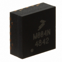
MMG3004NT1 Freescale Semiconductor, MMG3004NT1 Datasheet - Page 20

MMG3004NT1
Manufacturer Part Number
MMG3004NT1
Description
IC AMP RF GP 2200MHZ 5V 16-PQFN
Manufacturer
Freescale Semiconductor
Specifications of MMG3004NT1
Current - Supply
250mA
Frequency
400MHz ~ 2.2GHz
Gain
16dB
Noise Figure
3.4dB
P1db
27dBm
Package / Case
16-PQFN, 16-PowerQFN
Rf Type
Cellular, PCS, PHS, WLL
Test Frequency
2.14GHz
Voltage - Supply
5V
Manufacturer's Type
Broadband Amplifier
Number Of Channels
1
Supply Current
275@5VmA
Frequency (max)
2.2GHz
Operating Supply Voltage (typ)
5V
Operating Supply Voltage (max)
6V
Package Type
Power QFN EP
Mounting
Surface Mount
Pin Count
16
Noise Figure (typ)
3.4@2140MHzdB
Noise Figure Typ
3.4dB
Rf Ic Case Style
PQFN
No. Of Pins
16
Operating Temperature Range
-65°C To +150°C
Frequency Max
2.2GHz
Filter Terminals
SMD
Rohs Compliant
Yes
Rf Transistor Case
PQFN
Peak Reflow Compatible (260 C)
Yes
Leaded Process Compatible
Yes
Output Third Order Intercept Point, Ip3
44dB
Lead Free Status / RoHS Status
Lead free / RoHS Compliant
Other names
MMG3004NT1
MMG3004NT1TR
MMG3004NT1TR
Available stocks
Company
Part Number
Manufacturer
Quantity
Price
Part Number:
MMG3004NT1
Manufacturer:
FREESCALE
Quantity:
20 000
20
Application Notes
• AN1955: Thermal Measurement Methodology of RF Power Amplifiers
• AN3100: General Purpose Amplifier Biasing
• AN3778: PCB Layout Guidelines for PQFN/QFN Style Packages Requiring Thermal Vias for Heat Dissipation
Software
• .s2p File
Development Tools
• Printed Circuit Boards
For Software and Tools, do a Part Number search at http://www.freescale.com, and select the “Part Number” link. Go to the
Software & Tools tab on the part’s Product Summary page to download the respective tool.
MMG3004NT1
Revision
Refer to the following documents to aid your design process.
The following table summarizes revisions to this document.
2
3
4
5
June 2009
Mar. 2007
Mar. 2008
May 2010
Date
• Corrected Fig. 24, Single--Carrier W--CDMA Adjacent Channel Power Ratio versus Output Power y--axis
• Replaced Case Outline 1543--02 with updated 1543--03, Issue C, p. 1, 16--18
• Added V
• Updated Part Numbers in Table 8, Component Designations and Values, 900 MHz, to RoHS compliant part
• Corrected circuit board callouts, V
• Removed I
• Updated Part Numbers in Table 9, Component Designations and Values, 1900--2200 MHz, to RoHS compliant
• Corrected circuit board callouts, V
• Removed I
• Replaced Table 10, S--Parameters, p. 13--15
• Added Product Documentation and Revision History, p. 19
• Corrected Tape and Reel information from 12 mm, 7 inch Reel to 16 mm, 13 inch Reel, p. 1
• Removed Footnote 2, Continuous voltage and current applied to device, from Table 2, Maximum Ratings, p. 1
• Corrected S--Parameter table frequency column label to read “MHz” versus “GHz” and corrected frequency
• Replaced Case Outline 1543--03, Issue C, with 1543--04, Issue D, p. 1, 17--19. Corrected I/O dimension from
• Corrected temperature at which ThetaJC is measured from 25°C to 88°C, Thermal Characteristics table, p. 1
• Replaced Figs. 12 and 22, IS--95 Adjacent Channel Power Ratio versus Output Power, with revised graphs,
• Changed Thermal Characteristics table values for Thermal Resistance from 33 to 23.2 as a result of an
• Added new Fig. 3, Third Order Output Intercept Point versus Output Power and Supply Current, p. 4
• Added AN3778, PCB Layout Guidelines for PQFN/QFN Style Packages Requiring Thermal Vias for Heat
• Added .s2p File availability to Product Software, p. 20
numbers, p. 5
Layout, 900 MHz, p. 6
versus Output Power, 900 MHz, p. 8
part numbers, p. 9
Layout, 1900--2200 MHz, p. 10
versus Output Power, 1900--2200 MHz, and Fig. 24, Single--Carrier W--CDMA Adjacent Channel Power Ratio
versus Output Power, 1900--2200 MHz, p. 12
(ACPR) unit of measure to dBc, p. 12
values from GHz to MHz, p. 13, 14, 15
0.95--1.2 mm to 0.925--1.175 mm.
p. 8, 12
improvement made in the thermal measurement method. I
changed from 88°C to 90°C , p. 1
Dissipation, Application Notes, p. 20
PRODUCT DOCUMENTATION, SOFTWARE AND TOOLS
CC
DC
DC
callout to Pin Connections 10, 11, and 12 in Fig. 1, Pin Connections, p. 3
value due to its variability over temperature, Figs. 12--13, IS--95 Adjacent Channel Power Ratio
value due to its variability over temperature, Figs. 22--23, IS--95 Adjacent Channel Power Ratio
REVISION HISTORY
p
p
to V
to V
BA
BA
and V
and V
Description
CC
CC
to V
to V
SUPPLY
SUPPLY
DC
changed from 250 mA to 260 mA and T
, Fig. 5, 50 Ohm Test Circuit Component
, Fig. 15, 50 Ohm Test Circuit Component
Freescale Semiconductor
RF Device Data
(continued)
C


