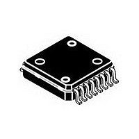
MHVIC2114NR2 Freescale Semiconductor, MHVIC2114NR2 Datasheet

MHVIC2114NR2
Specifications of MHVIC2114NR2
Available stocks
Related parts for MHVIC2114NR2
MHVIC2114NR2 Summary of contents
Page 1
... Technical Data RF LDMOS Wideband Integrated Power Amplifier The MHVIC2114NR2 wideband integrated circuit is designed for base station applications. It uses Freescale’s newest High Voltage ( Volts) LDMOS IC technology and integrates a multi - stage structure. Its wideband On - Chip matching design makes it usable from 1600 to 2600 MHz. The linearity performances cover all modulation formats for cellular applications: CDMA and W - CDMA ...
Page 2
... MHz, Single - Carrier W - CDMA, 3.84 MHz Channel Bandwidth Carrier. ACPR measured in 3.84 MHz Channel out Bandwidth @ ±5 MHz Offset. PAR = 8 0.01% Probability on CCDF. Power Gain Gain Flatness Input Return Loss Adjacent Channel Power Ratio Group Delay Phase Linearity MHVIC2114NR2 2 Stage 1, 27 Vdc DQ1 Stage 2, 27 Vdc 204 mA DQ2 Stage 3, 27 Vdc, I ...
Page 3
... V DS2 + + C13 C12 C11 Figure 3. MHVIC2114NR2 Test Circuit Schematic Table 6. MHVIC2114NR2 Test Circuit Component Designations and Values Part C1, C5, C8, C12, C14, C19 1 μF Tantalum Chip Capacitors C2, C3, C4, C7, C11, C18 0.01 μF Chip Capacitors C6, C10, C17 6.8 pF Chip Capacitors (ACCU - ...
Page 4
... Freescale has begun the transition of marking Printed Circuit Boards (PCBs) with the Freescale Semiconductor signature/logo. PCBs may have either Motorola or Freescale markings during the transition period. These changes will have no impact on form, fit or function of the current product. Figure 4. MHVIC2114NR2 Test Circuit Component Layout MHVIC2114NR2 4 V ...
Page 5
... Figure 6. Delay versus Frequency = 27 Vdc dBm CW out = 96 mA 204 mA 111 mA DQ2 DQ3 T = 85_C C 2110 2120 2130 2140 2150 2160 f, FREQUENCY, (MHz −30_C Vdc 2140 MHz = 96 mA 204 mA 111 mA DQ2 DQ3 OUTPUT POWER (dBm) out MHVIC2114NR2 = 85_C C 25_C 2170 2180 2170 2180 25_C 85_C ...
Page 6
... Figure 13. Two - Tone Intermodulation Distortion Products versus Tone Spacing 4.5 4.4 4.3 4.2 4 3.9 3.8 3.7 I GS3 3.6 3.5 −40 MHVIC2114NR2 6 TYPICAL CHARACTERISTICS − Vdc DD − dBm Two−Tone Avg. out Tone Spacing = 100 kHz −40 −50 −60 −70 2140 MHz − ...
Page 7
... Z = Device input impedance as measured from in gate to ground Test circuit impedance as measured load from drain to ground. Output Device Matching Under Test Network load f = 2110 MHz 2170 MHz = 23 dBm out load Ω MHVIC2114NR2 7 ...
Page 8
... MHVIC2114NR2 8 NOTES RF Device Data Freescale Semiconductor ...
Page 9
... RF Device Data Freescale Semiconductor NOTES MHVIC2114NR2 9 ...
Page 10
... MHVIC2114NR2 10 NOTES RF Device Data Freescale Semiconductor ...
Page 11
... A1 0.025 0.100 A2 1.950 2.100 D 6.950 7.100 D1 4.372 5.180 E 8.850 9.150 E1 6.950 7.100 E2 4.372 5.180 L 0.466 0.720 L1 0.250 BSC b 0.300 0.432 b1 0.300 0.375 c 0.180 0.279 c1 0.180 0.230 e 0.800 BSC h −−− 0.600 aaa 0.200 bbb 0.200 ccc 0.100 MHVIC2114NR2 11 ...
Page 12
... RoHS- compliant and/or non - Pb- free counterparts. For further information, see http://www.freescale.com or contact your Freescale sales representative. For information on Freescale’s Environmental Products program http://www.freescale.com/epp. MHVIC2114NR2 Document Number: MHVIC2114NR2 Rev. 5, 5/2006 12 RoHS-compliant and/or Pb- free versions of Freescale products have the functionality and electrical characteristics of their non-RoHS-compliant and/or non-Pb- free counterparts ...


