MW6IC2015NBR1 Freescale Semiconductor, MW6IC2015NBR1 Datasheet
MW6IC2015NBR1
Specifications of MW6IC2015NBR1
Available stocks


Related parts for MW6IC2015NBR1

MW6IC2015NBR1 Summary of contents
Page 1
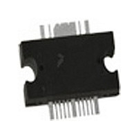
... CASE 1329 - 272 PLASTIC MW6IC2015NBR1 CASE 1329A - 272 GULL PLASTIC MW6IC2015GNBR1 GND 1 16 GND V 2 DS1 out in V DS2 GS1 V 9 GS2 GND 11 GND (Top View) Note: Exposed backside of the package is the source terminal for the transistors. Figure 2. Pin Connections MW6IC2015NBR1 MW6IC2015GNBR1 1 ...
Page 2
... Continuous use at maximum temperature will affect MTTF. 2. MTTF calculator available at http://www.freescale.com/rf. Select Software & Tools/Development Tools/Calculators to access MTTF calculators by product. 3. Refer to AN1955, Thermal Measurement Methodology of RF Power Amplifiers http://www.freescale.com/rf. Select Documentation/Application Notes - AN1955. MW6IC2015NBR1 MW6IC2015GNBR1 2 Stage 1, 26 Vdc 100 mA DQ1 ...
Page 3
... Vdc 130 mA 170 mA, DD DQ1 DQ2 — 27 — — 19 — — 0.8 — — — — — MW6IC2015NBR1 MW6IC2015GNBR1 Unit ° ns ° dBc dBc 3 ...
Page 4
... Z4 0.13″ x 0.35″ Microstrip Z5 0.10″ x 0.35″ Microstrip Figure 3. MW6IC2015NBR1(GNBR1) Test Circuit Schematic — 1930 - 1990 MHz Table 6. MW6IC2015NBR1(GNBR1) Test Circuit Component Designations and Values — 1930 - 1990 MHz Part C1, C14, C15 2.2 μF Chip Capacitors C2, C4, C11 5.6 pF Chip Capacitors C3 μ ...
Page 5
... V DD1 MW6IC2015, Rev. 0 C14 R1 V GG1 R2 C15 V GG2 Figure 4. MW6IC2015NBR1(GNBR1) Test Circuit Component Layout — 1930 - 1990 MHz RF Device Data Freescale Semiconductor C11 C6 C8 C10 DD2 C9 C12 C13 C5 MW6IC2015NBR1 MW6IC2015GNBR1 5 ...
Page 6
... DQ2 Vdc DD Center Frequency = 1960 MHz 24 100 kHz Tone Spacing 23 0 OUTPUT POWER (WATTS) AVG. out Figure 7. Two - Tone Power Gain versus Output Power MW6IC2015NBR1 MW6IC2015GNBR1 6 PAE G ps IRL IMD Vdc 7.5 W (Avg.) DD out I = 100 mA 170 mA DQ1 DQ2 100 kHz Tone Spacing ...
Page 7
... Figure 13. Power Gain versus Output Power Ideal Actual Vdc 100 mA 170 mA DQ1 DQ2 Pulsed CW, 8 μsec(on), 1 msec(off 1960 MHz INPUT POWER (dBm) in Input Power −25 −30 G −35 ps −40 −45 −50 −55 − 100 mA DQ1 I = 170 mA DQ2 f = 1840 MHz OUTPUT POWER (WATTS) CW out MW6IC2015NBR1 MW6IC2015GNBR1 ...
Page 8
... DQ1 I = 170 mA 8 DQ2 f = 1960 MHz EDGE Modulation 6 PAE OUTPUT POWER (WATTS) AVG. out Figure 16. EVM and Power Added Efficiency versus Output Power MW6IC2015NBR1 MW6IC2015GNBR1 8 − −15 28 −20 26 − DQ1 Two−Tone Measurements, Center Frequency = 1960 MHz 22 −30 2050 2100 ...
Page 9
... Figure 18. MTTF versus Junction Temperature GSM TEST SIGNAL Reference Power VBW = 30 kHz Sweep Time = 70 ms RBW = 30 kHz 400 kHz 600 kHz Center 1.96 GHz 200 kHz Figure 19. EDGE Spectrum 210 230 250 400 kHz 600 kHz Span 2 MHz MW6IC2015NBR1 MW6IC2015GNBR1 9 ...
Page 10
... MHz f = 1990 MHz Figure 20. Series Equivalent Source and Load Impedance — 1930 - 1990 MHz MW6IC2015NBR1 MW6IC2015GNBR1 10 Z load = 25 Ω Vdc 100 mA 170 mA DQ1 DQ2 out source MHz W 1930 23.37 - j21.93 1.62 + j0.26 1950 22.77 - j22.53 1.59 + j0.04 1970 22.19 - j22.20 1 ...
Page 11
... Z5 0.10″ x 0.35″ Microstrip Z6* 0.26″ x 0.04″ Microstrip Figure 21. MW6IC2015NBR1(GNBR1) Test Circuit Schematic — 1805 - 1880 MHz Table 7. MW6IC2015NBR1(GNBR1) Test Circuit Component Designations and Values — 1805 - 1880 MHz Part C1, C14, C15 2.2 μF Chip Capacitors C2, C4, C11 5.6 pF Chip Capacitors C3 μ ...
Page 12
... V DD1 MW6IC2015, Rev. 0 C14 R1 V GG1 R2 C15 V GG2 Figure 22. MW6IC2015NBR1(GNBR1) Test Circuit Component Layout — 1805 - 1880 MHz MW6IC2015NBR1 MW6IC2015GNBR1 DD2 C9 C11 C16 C12 C13 C10 Device Data Freescale Semiconductor ...
Page 13
... Figure 26. Intermodulation Distortion 0 IRL −10 −20 PAE −30 IMD − −50 −60 1900 0 −12 −24 = 170 mA −36 −48 −60 1880 3rd Order = 170 mA DQ2 5th Order 7th Order OUTPUT POWER (WATTS) PEP out Products versus Output Power MW6IC2015NBR1 MW6IC2015GNBR1 30 13 ...
Page 14
... PAE 26 85_C Vdc 170 mA 1840 MHz DQ2 22 0 OUTPUT POWER (WATTS) CW out Figure 30. Power Gain and Power Added Efficiency versus CW Output Power MW6IC2015NBR1 MW6IC2015GNBR1 14 48 P3dB = 44.7 dBm ( P1dB = 44 dBm ( 100 10 Figure 28. Pulsed CW Output Power versus Vdc 100 mA 170 mA DQ1 ...
Page 15
... W (Avg.) out = 100 mA 170 mA DQ2 1800 1820 1840 1860 1880 f, FREQUENCY (MHz) Figure 33. Power Gain versus Frequency = 26 Vdc T = 25_C C = 100 mA 170 mA DQ2 −30_C 85_C 85_C OUTPUT POWER (WATTS) AVG. out versus Output Power MW6IC2015NBR1 MW6IC2015GNBR1 1900 1920 −30_C 25_C 30 15 ...
Page 16
... MHz f = 1880 MHz Z load Figure 36. Series Equivalent Source and Load Impedance — 1805 - 1880 MHz MW6IC2015NBR1 MW6IC2015GNBR1 Ω 1880 MHz Z source f = 1800 MHz Vdc 130 mA 170 mA DQ1 DQ2 out source MHz W 1800 24.32 - j26.99 1.94 - j1.29 1820 23.96 - j25.93 1.88 - j1.42 1840 23 ...
Page 17
... Microstrip Z4 0.148″ x 0.237″ Microstrip Z5 0.064″ x 0.237″ Microstrip Figure 37. MW6IC2015NBR1(GNBR1) Test Circuit Schematic — SCDMA Table 8. MW6IC2015NBR1(GNBR1) Test Circuit Component Designations and Values — SCDMA Part C1, C3, C5, C14 2.2 μF Chip Capacitors C2, C4, C10 5.6 pF Chip Capacitors ...
Page 18
... C1 MW6IC2015NB, Rev. 1 C12 C13 R1 R2 Figure 38. MW6IC2015NBR1(GNBR1) Test Circuit Component Layout — SCDMA MW6IC2015NBR1 MW6IC2015GNBR1 DD1 C6 C14 V GG DD2 C11 C10 Device Data Freescale Semiconductor ...
Page 19
... Alt−L 1.5 1 Adj−U 0 1.28 MHz Channel BW VBW = 300 kHz Sweep Time = 200 ms RBW = 30 kHz +ALT2 in 1.28 MHz BW +3.2 MHz Offset −ALT1 in +ALT1 in 1.28 MHz BW 1.28 MHz BW −1.6 MHz Offset +1.6 MHz Offset 2.5 MHz Span 25 MHz f, FREQUENCY (MHz) MW6IC2015NBR1 MW6IC2015GNBR1 19 ...
Page 20
... Z load f = 2070 MHz f = 1950 MHz Figure 43. Series Equivalent Input and Load Impedance — SCDMA MW6IC2015NBR1 MW6IC2015GNBR1 Ω source f = 2070 MHz f = 1950 MHz Vdc 150 mA 160 mA DD DQ1 DQ2 source load MHz W W 1950 25.25 + j0.19 1.78 + j0.33 1960 25.16 + j0.34 1.75 + j0.43 1970 25 ...
Page 21
... RF Device Data Freescale Semiconductor PACKAGE DIMENSIONS MW6IC2015NBR1 MW6IC2015GNBR1 21 ...
Page 22
... MW6IC2015NBR1 MW6IC2015GNBR1 22 RF Device Data Freescale Semiconductor ...
Page 23
... RF Device Data Freescale Semiconductor MW6IC2015NBR1 MW6IC2015GNBR1 23 ...
Page 24
... MW6IC2015NBR1 MW6IC2015GNBR1 24 RF Device Data Freescale Semiconductor ...
Page 25
... RF Device Data Freescale Semiconductor MW6IC2015NBR1 MW6IC2015GNBR1 25 ...
Page 26
... MW6IC2015NBR1 MW6IC2015GNBR1 26 RF Device Data Freescale Semiconductor ...
Page 27
... BSC to 0.25 BSC. Added JEDEC Standard Package Number. • Replaced Case Outline 1329 - 09, Issue L, with 1329 - 09, Issue 23. Added pin numbers 1 through 17. RF Device Data Freescale Semiconductor PRODUCT DOCUMENTATION REVISION HISTORY Description and V callouts, Figs. 3 and 21, Test Circuit Schematic 11, Figs. 4 and 22, Test BIAS SUPPLY 2 and listed MW6IC2015NBR1 MW6IC2015GNBR1 27 ...
Page 28
... P.O. Box 5405 Denver, Colorado 80217 1 - 800 - 441 - 2447 303 - 675 - 2140 Fax 303 - 675 - 2150 LDCForFreescaleSemiconductor@hibbertgroup.com MW6IC2015NBR1 MW6IC2015GNBR1 Document Number: MW6IC2015N Rev. 3, 12/2008 28 Information in this document is provided solely to enable system and software implementers to use Freescale Semiconductor products. There are no express or implied copyright licenses granted hereunder to design or fabricate any integrated circuits or integrated circuits based on the information in this document ...