AD8354ACP-R2 Analog Devices Inc, AD8354ACP-R2 Datasheet - Page 15
AD8354ACP-R2
Manufacturer Part Number
AD8354ACP-R2
Description
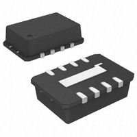
IC RF GAIN BLOCK 8-LFCSP
Manufacturer
Analog Devices Inc
Datasheet
1.AD8354ACPZ-REEL7.pdf
(16 pages)
Specifications of AD8354ACP-R2
Rohs Status
RoHS non-compliant
Current - Supply
16mA ~ 31mA
Frequency
1MHz ~ 2.7GHz
Gain
17.1dB
Noise Figure
5.4dB
Package / Case
8-LFCSP
Rf Type
Cellular, LMDS, MMDS
Test Frequency
2.7GHz
Voltage - Supply
3V, 5V
P1db
-
Other names
AD8354ACP-R2CT


EVALUATION BOARD
Figure 40 shows the schematic of the AD8354 evaluation board.
Note that L1 is shown as an optional component that is used to
obtain maximum gain only when V
by a single supply in the 2.7 V to 5.5 V range. The power supply
is decoupled by a 0.47 μF and a 100 pF capacitor.
INPUT
Table 5. Evaluation Board Configuration Options
Component
C1, C2
C3
C4
L1
1000pF
C1
Figure 40. Evaluation Board Schematic
Function
AC coupling capacitors.
High frequency bypass capacitor.
Low frequency bypass capacitor.
Optional RF choke, used to increase
current through output stage when
V
when V
P
1
2
3
4
= 3 V. Not recommended for use
NC = NO CONNECT
COM1
NC
INPT
COM2
P
AD8354
= 5 V.
VOUT
COM1
COM2
VPOS
P
= 3 V. The board is powered
8
7
6
5
L1
1000pF
C3
100pF
C2
Default
Value
1000 pF,
0603
100 pF,
0603
0.47 μF,
0603
100 nH,
0603
OUTPUT
C4
0.47μF
Rev. D | Page 15 of 16
Figure 42. Component Side
Figure 41. Silkscreen Top
AD8354
Related parts for AD8354ACP-R2
Image
Part Number
Description
Manufacturer
Datasheet
Request
R

Part Number:
Description:
250 MHz, Voltage Output 4-Quadrant Multiplier
Manufacturer:
Analog Devices
Datasheet:

Part Number:
Description:
±1.7g Dual-Axis IMEMS Accelerometer Evaluation Board
Manufacturer:
Analog Devices Inc
Datasheet:

Part Number:
Description:
Inertial Sensor Evaluation System
Manufacturer:
Analog Devices Inc
Datasheet:
Part Number:
Description:
Manufacturer:
Analog Devices Inc
Datasheet:
Part Number:
Description:
Manufacturer:
Analog Devices Inc
Datasheet:
Part Number:
Description:
Manufacturer:
Analog Devices Inc
Datasheet:
Part Number:
Description:
Manufacturer:
Analog Devices Inc
Datasheet:
Part Number:
Description:
Manufacturer:
Analog Devices Inc
Datasheet:
Part Number:
Description:
Manufacturer:
Analog Devices Inc
Datasheet:
Part Number:
Description:
Manufacturer:
Analog Devices Inc
Datasheet:
Part Number:
Description:
Manufacturer:
Analog Devices Inc
Datasheet:
Part Number:
Description:
Manufacturer:
Analog Devices Inc
Datasheet:
Part Number:
Description:
Manufacturer:
Analog Devices Inc
Datasheet: