RF2483PCK-410 RFMD, RF2483PCK-410 Datasheet - Page 8
RF2483PCK-410
Manufacturer Part Number
RF2483PCK-410
Description
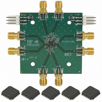
KIT EVAL FOR RF2483
Manufacturer
RFMD
Type
Modulatorr
Datasheet
1.RF2483PCK-410.pdf
(28 pages)
Specifications of RF2483PCK-410
Frequency
700MHz ~ 2.4GHz
For Use With/related Products
RF2483
Lead Free Status / RoHS Status
Lead free / RoHS Compliant
Other names
689-1040
Available stocks
Company
Part Number
Manufacturer
Quantity
Price
Company:

Part Number:
RF2483PCK-410
Manufacturer:
RFMD
Quantity:
5 000


RF2483
8 of 28
Pin
1
2
3
4
5
6
Function
ENABLE
ISIG N
ISIG P
VCC3
VCC2
VCC1
Description
Supply for RF output circuits.
Supply for modulator and biasing circuits.
In phase I channel positive baseband input port. Best performance is
achieved when the ISIGP and ISIGN are driven differentially. The recom-
mended CW differential drive level (V
This input should be DC-biased at 1.2V±0.05V. The common-mode DC
coltage on the ISIGP and ISIGN input signals is used to bias the modulator.
In sleep mode an internal FET switch is opened, the input goes high imped-
ance and the modulator is de-biased. The input impedance is typically
5.5kΩ at low frequencies and at higher frequencies can be modeled as
50Ω in series with 12pF to ground.
Phase or amplitude errors between the ISIGP and ISIGN signals may result
in the even order distortion of the modulation in the output spectrum.
DC offsets between the ISIGP and ISIGN signals will result in increased car-
rier leakage. Small DC offsets may be deliberately applied between the
ISIGP/ISIGN and QSIGP/QSIGN inputs to cancel out LO leakage. The opti-
mum corrective DC offsets will change with mode, frequency and gain con-
trol.
Common-mode noise on the ISIGP and ISGN should be kept low as it may
degrade the noise performance of the modulator.
Phase offsets may be applied between the I and Q channels to improve the
sideband suppression performance.
In phase I channel negative baseband input port. See ISIGP.
Enables power to the device.
CMOS input.
Logic 1 (1.4V to VCC)=Enabled.
Logic 0 (0V to 0.5V)=Powered Down.
Supply for the LO buffers and quadrature network.
The sideband suppression is a function of the VCC1 voltage. The inclusion
of R3 (39Ω) lowers the voltage on VCC1 by around 400mV and results an
improvement in sideband suppression but around a 0.2dB increase in
noise at 20MHz offset.
7628 Thorndike Road, Greensboro, NC 27409-9421 · For sales or technical
support, contact RFMD at (+1) 336-678-5570 or sales-support@rfmd.com.
ISIGP
-V
ISIGN
) is 800mV
P-P
.
Interface Schematic
VCC3
VCC2
GND1
VCC1
Modulator and
V
LO Quadrature
V
Generator and
RF Output
C C 2
C C 2
Amplifier
VGA
Buffers
5 0 Ω
V
5 0 Ω
C C 2
Rev A9 DS080403
1 2 p F
1 2 p F
VCC2
Related parts for RF2483PCK-410
Image
Part Number
Description
Manufacturer
Datasheet
Request
R

Part Number:
Description:
IC AMP HBT GAAS CATV 8-SOIC
Manufacturer:
RFMD
Datasheet:

Part Number:
Description:
IC AMP MMIC GAAS 12GHZ 4-MICROX
Manufacturer:
RFMD
Datasheet:

Part Number:
Description:
IC AMP 3V LOW-NOISE SOT23-6
Manufacturer:
RFMD
Datasheet:

Part Number:
Description:
KIT EVAL FOR NBB-310
Manufacturer:
RFMD
Datasheet:
Part Number:
Description:
IC AMPLIFIER MMIC LNA 8-QFN
Manufacturer:
RFMD
Datasheet:
Part Number:
Description:
IC AMP MMIC GAAS 4GHZ 4-MICROX
Manufacturer:
RFMD
Datasheet:
Part Number:
Description:
IC SWITCH 10W PHEMT SPDT 12QFN
Manufacturer:
RFMD
Datasheet:
Part Number:
Description:
IC QUADRATURE MODULATOR 16-SOIC
Manufacturer:
RFMD
Datasheet:
Part Number:
Description:
100MHZ TO 4000MHZ, GAAS PHEMT MMIC LOW NOISE AMPLIFIERS
Manufacturer:
RFMD
Part Number:
Description:
KIT EVAL FOR RF2336
Manufacturer:
RFMD
Datasheet:


Part Number:
Description:
IC AMP WLAN/LNA DVR 3V SOT23-5
Manufacturer:
RFMD
Datasheet:

Part Number:
Description:
IC AMP HBT GAAS LNA BYPASS 8-QFN
Manufacturer:
RFMD
Datasheet:

Part Number:
Description:
IC AMP MMIC GAAS 10GHZ 4-MICROX
Manufacturer:
RFMD
Datasheet: