XE1205SKC433XE1 Semtech, XE1205SKC433XE1 Datasheet - Page 38
XE1205SKC433XE1
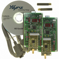
Manufacturer Part Number
XE1205SKC433XE1
Description
KIT STARTER FOR XE1205 433MHZ
Manufacturer
Semtech
Series
TrueRF™r
Type
Transceiver, ISMr
Specifications of XE1205SKC433XE1
Frequency
433MHz
For Use With/related Products
XE1205 (433MHz)
Lead Free Status / RoHS Status
Contains lead / RoHS non-compliant


Figure 23 illustrates the switching time between two carrier frequencies in receive mode. TS_RFSW is defined as the
switching
the boost process is used (Init_filter set to “11”).
Figure 24 shows the switch
switching time of the frequency synthesizer and the time required by the power amplifier to reach the steady-state
operating conditions.
7.3.2
If MCParam_Select_mode is high then the trans
MCParam_Chip_mode can be used in read mode but has no effect on the transceiver mode.
The refer
external 39 MHz quartz crystal or a TCXO or an external clock. If an external clock is used, the register OSCParam_Osc
has to be set high, and the 39 MHz clock signal should to be supplied to the pin “XTA” and the pin “XTB” should be left
open. If a TCXO is used, its output signal should be connected to the pin “XTA” and the pin “XTB” should be left.
T
overtone operation requires an internal resistor to be connected in parallel with the crystal. This resistor can be
connected by programming the register OSCParam_Resxosc(3:0). The required value depends on the crystal
© Semtech 2008
he transceiver can be used with a 39 MHz fundamental mode quartz crystal or with a 3
7.4
Programmed frequency
NSS_CONFIG
A
Programmed frequency
NSS_CONFIG
A
Actual mode
Actual mode
ctual frequency
ctual frequency
ence clock used for the frequency synthesizer and t
XE1205 switching time using SW(1:0) pins.
SELECTION OF THE REFERENCE FREQUENCY
time of the frequency synthesizer and the time needed by the base band filter to reach the steady-state when
Figure 24. Switching between two carrier frequencies in transmit mode.
Figure 23. Switching between two carrier frequencies in receive mode.
ing time between two carrier frequencies in transmit mode. TS
f1
f1
f1
f1
transmit
receive
ceiver mode is fixed by SW(1:0) pins and register
38
he internal digital circuitry may be generated by either an
TS_RFSW
TS_TFSW
f2
f2
f2
f2
_TFSW is defined as the
rd
overtone crystal. Third
XE1205
www.semtech.com
Related parts for XE1205SKC433XE1
Image
Part Number
Description
Manufacturer
Datasheet
Request
R

Part Number:
Description:
Low-power, High Link Budget Integrated Uhf Transceiver
Manufacturer:
Semtech Corporation
Datasheet:

Part Number:
Description:
EVALUATION BOARD
Manufacturer:
Semtech
Datasheet:
Part Number:
Description:
EVALUATION BOARD
Manufacturer:
Semtech
Datasheet:
Part Number:
Description:
VOLTAGE SUPPRESSOR, TRANSIENT SEMTECH
Manufacturer:
Semtech
Datasheet:
Part Number:
Description:
HIGH VOLTAGE CAPACITORS MONOLITHIC CERAMIC TYPE
Manufacturer:
Semtech Corporation
Datasheet:
Part Number:
Description:
EZ1084CM5.0 AMP POSITIVE VOLTAGE REGULATOR
Manufacturer:
Semtech Corporation
Datasheet:
Part Number:
Description:
3.0 AMP LOW DROPOUT POSITIVE VOLTAGE REGULATORS
Manufacturer:
Semtech Corporation
Datasheet:
Part Number:
Description:
Manufacturer:
Semtech Corporation
Datasheet:
Part Number:
Description:
RailClamp Low Capacitance TVS Diode Array
Manufacturer:
Semtech Corporation
Datasheet:
Part Number:
Description:
Manufacturer:
Semtech Corporation
Datasheet:
Part Number:
Description:
Manufacturer:
Semtech Corporation
Datasheet:
Part Number:
Description:
Manufacturer:
Semtech Corporation
Datasheet: