NLB-400-PCK RFMD, NLB-400-PCK Datasheet - Page 2
NLB-400-PCK
Manufacturer Part Number
NLB-400-PCK
Description
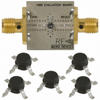
KIT EVAL FOR NLB-400
Manufacturer
RFMD
Type
Amplifierr
Datasheet
1.NLB-400-T1.pdf
(8 pages)
Specifications of NLB-400-PCK
Frequency
0Hz ~ 6GHz
For Use With/related Products
NLB-400
Lead Free Status / RoHS Status
Lead free / RoHS Compliant
Other names
689-1061
Available stocks
Company
Part Number
Manufacturer
Quantity
Price
Company:

Part Number:
NLB-400-PCK
Manufacturer:
RFMD
Quantity:
5 000


3
NLB-400
3-24
Absolute Maximum Ratings
RF Input Power
Power Dissipation
Device Current
Channel Temperature
Operating Temperature
Storage Temperature
Exceeding any one or a combination of these limits may cause permanent
damage.
Overall
Small Signal Power Gain, S21
Gain Flatness, GF
Input VSWR
Output VSWR
Bandwidth, BW
Output Power @
Noise Figure, NF
Third Order Intercept, IP3
Reverse Isolation, S12
Device Voltage, V
Gain Temperature Coefficient,
MTTF versus Temperature
@ I
Case Temperature
Junction Temperature
MTTF
Thermal Resistance
θ
JC
CC
-1dB Compression, P1dB
δG
=50mA
T
/δT
Parameter
Parameter
D
7628 Thorndike Road, Greensboro, NC 27409-9421 · For sales or technical
support, contact RFMD at (+1) 336-678-5570 or sales-support@rfmd.com.
Min.
16.0
10.8
3.6
-65 to +150
-45 to +85
Rating
Specification
+20
300
200
70
>1,000,000
-0.0015
1.65:1
1.65:1
1.75:1
±0.65
+29.6
+27.3
Typ.
1.5:1
1.9:1
2.2:1
13.0
11.5
12.0
14.6
17.0
119
185
4.7
4.1
-18
3.9
85
Max.
Unit
dBm
mW
4.2
mA
°C
°C
°C
dB/°C
hours
°C/W
Unit
dBm
dBm
dBm
The information in this publication is believed to be accurate and reliable. How-
ever, no responsibility is assumed by RF Micro Devices, Inc. ("RFMD") for its use,
nor for any infringement of patents, or other rights of third parties, resulting
from its use. No license is granted by implication or otherwise under any patent
or patent rights of RFMD. RFMD reserves the right to change component cir-
cuitry, recommended application circuitry and specifications at any time without
prior notice.
RoHS status based on EUDirective2002/95/EC (at time of this document revi-
sion).
GHz
dB
dB
dB
dB
dB
dB
°C
°C
V
V
f=0.1GHz to 1.0GHz
f=1.0GHz to 4.0GHz
f=4.0GHz to 6.0GHz
f=0.1GHz to 2.0GHz
f=0.1GHz to 4.0GHz
f=4.0GHz to 6.0GHz
f=6.0GHz to 10.0GHz
f=0.1GHz to 4.0GHz
f=4.0GHz to 6.0GHz
f=6.0GHz to 10.0GHz
BW3 (3dB)
f=2.0GHz
f=6.0GHz
f=3.0GHz
f=2.0GHz
f=6.0GHz
f=0.1GHz to 12.0GHz
J
-------------------------- -
D
T
Caution! ESD sensitive device.
V
=+3.9V, I
–
D
T
⋅
CASE
I
CC
CC
=47mA, Z
=
Condition
θ
JC
(
0
°C Watt
=50Ω, T
Rev A10 DS070123
⁄
A
=+25°C
)
Related parts for NLB-400-PCK
Image
Part Number
Description
Manufacturer
Datasheet
Request
R

Part Number:
Description:
IC AMP MMIC GAAS 6GHZ 4-MICROX
Manufacturer:
RFMD
Datasheet:
Part Number:
Description:
IC AMP MMIC GAAS 10GHZ 4-MICROX
Manufacturer:
RFMD
Datasheet:
Part Number:
Description:
IC AMP MMIC GAAS 10GHZ 4-MICROX
Manufacturer:
RFMD
Datasheet:

Part Number:
Description:
KIT EVAL FOR NLB-310
Manufacturer:
RFMD
Datasheet:

Part Number:
Description:
KIT EVAL FOR NLB-300
Manufacturer:
RFMD
Datasheet:


Part Number:
Description:
IC AMP HBT GAAS CATV 8-SOIC
Manufacturer:
RFMD
Datasheet:

Part Number:
Description:
IC AMP MMIC GAAS 12GHZ 4-MICROX
Manufacturer:
RFMD
Datasheet:

Part Number:
Description:
IC AMP 3V LOW-NOISE SOT23-6
Manufacturer:
RFMD
Datasheet:

Part Number:
Description:
KIT EVAL FOR NBB-310
Manufacturer:
RFMD
Datasheet:
Part Number:
Description:
IC AMPLIFIER MMIC LNA 8-QFN
Manufacturer:
RFMD
Datasheet:
Part Number:
Description:
IC AMP MMIC GAAS 4GHZ 4-MICROX
Manufacturer:
RFMD
Datasheet:
Part Number:
Description:
IC SWITCH 10W PHEMT SPDT 12QFN
Manufacturer:
RFMD
Datasheet:
Part Number:
Description:
IC QUADRATURE MODULATOR 16-SOIC
Manufacturer:
RFMD
Datasheet:
Part Number:
Description:
100MHZ TO 4000MHZ, GAAS PHEMT MMIC LOW NOISE AMPLIFIERS
Manufacturer:
RFMD