1004-TCB1D434 Silicon Laboratories Inc, 1004-TCB1D434 Datasheet - Page 19
1004-TCB1D434
Manufacturer Part Number
1004-TCB1D434
Description
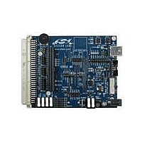
BOARD EVALUATION FOR SI1004
Manufacturer
Silicon Laboratories Inc
Type
Transceiver, ISMr
Specifications of 1004-TCB1D434
Mfg Application Notes
SI1000 Code Examples AppNote
Frequency
434MHz
Supply Voltage (min)
0.9 V
Product
RF Modules
Maximum Frequency
915 MHz
Output Power
13 dBm
Antenna
SMA
Supply Voltage (max)
3.6 V
For Use With/related Products
Si100x
Lead Free Status / RoHS Status
Lead free / RoHS Compliant
Lead Free Status / RoHS Status
Lead free / RoHS Compliant, Lead free / RoHS Compliant
Other names
336-1889


10.7. Target Board DEBUG Interface (J9)
The DEBUG connector J9 provides access to the DEBUG (C2) pins of the Si10xx. It is used to connect the Serial
Adapter or the USB Debug Adapter to the target board for in-circuit debugging and Flash programming. Table 3
shows the DEBUG pin definitions.
10.8. Serial Interface (J12)
A USB-to-UART bridge circuit (U3) and USB connector (P3) are provided on the target board to facilitate serial
connections to UART0 of the Si10xx. The Silicon Labs CP2103 (U3) USB-to-UART bridge provides data
connectivity between the Si10xx and the PC via a USB port. The VIO power supply and TX, RX, RTS and CTS
signals of UART0 may be connected to the CP2103 by installing shorting blocks on header J12. The shorting block
positions for connecting each of these signals to the CP2103 are listed in Table 4. To use this interface, the USB-
to-UART device drivers should be installed as described in Section 3.2. "CP210x USB to UART VCP Driver
Installation‚" on page 2.
10.9. Analog I/O (H1)
Several of the Si10xx target device’s port pins are connected to the H1 terminal block. Refer to Table 5 for the H1
terminal block connections.
Table 4. Serial Interface Header (J12) Description
Table 3. DEBUG Connector Pin Descriptions
Table 5. H1 Terminal Block Pin Descriptions
Header Pins UART0 Pin Description
2, 3, 9
Pin #
Pin #
J12[9–10]
J12[7–8]
J12[5–6]
J12[3–4]
J12[1–2]
10
1
4
5
6
7
8
1
2
3
4
P0.0/V
USB Power (+5 VDC from J9)
CP2103_VIO (VDD/DC+)
+3 VD (+3.3 VDC)
REF
Rev. 0.1
Not Connected
GND (Ground)
P0.6/CNVSTR
GND (Ground)
Description
Description
RST (Reset)
P0.7/IREF0
RST/C2CK
P2.7/C2D
TX_MCU (P0.5)
RX_MCU (P0.4)
(Voltage Reference)
P2.7
RTS (P0.6)
CTS (P0.7)
Si10xx-DK
19
Related parts for 1004-TCB1D434
Image
Part Number
Description
Manufacturer
Datasheet
Request
R


Part Number:
Description:
BOARD EVALUATION FOR SI1004
Manufacturer:
Silicon Laboratories Inc
Datasheet:

Part Number:
Description:
RF Connectors OSSM CABLE JACK STRT BULKHEAD
Manufacturer:
Tyco Electronics


Part Number:
Description:
SMD/C�/SINGLE-ENDED OUTPUT SILICON OSCILLATOR
Manufacturer:
Silicon Laboratories Inc
Part Number:
Description:
Manufacturer:
Silicon Laboratories Inc
Datasheet:
Part Number:
Description:
N/A N/A/SI4010 AES KEYFOB DEMO WITH LCD RX
Manufacturer:
Silicon Laboratories Inc
Datasheet:
Part Number:
Description:
N/A N/A/SI4010 SIMPLIFIED KEY FOB DEMO WITH LED RX
Manufacturer:
Silicon Laboratories Inc
Datasheet:
Part Number:
Description:
N/A/-40 TO 85 OC/EZLINK MODULE; F930/4432 HIGH BAND (REV E/B1)
Manufacturer:
Silicon Laboratories Inc
Part Number:
Description:
EZLink Module; F930/4432 Low Band (rev e/B1)
Manufacturer:
Silicon Laboratories Inc