MC1496PG ON Semiconductor, MC1496PG Datasheet
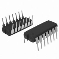
IC MOD/DEMODULTR BALANCED 14DIP

MC1496PG

Manufacturer Part Number
MC1496PG
Description
IC MOD/DEMODULTR BALANCED 14DIP
Manufacturer
ON Semiconductor
Datasheets

Specifications of MC1496PG

Function
Modulator/Demodulator
Frequency
300MHz
Rf Type
FM
Package / Case
14-DIP (0.300", 7.62mm)
Maximum Operating Temperature
+ 70 C
Maximum Power Dissipation
33 mW (Typ)
Minimum Operating Temperature
0 C
Modulation Type
Balanced
Mounting Style
Through Hole
Supply Current
0.005 A
Current, Supply
2 mA
Logic Function
Modulator/Demodulator
Package Type
PDIP-14
Temperature, Operating, Range
0 to +70 °C
Voltage, Supply
12 VDC
Supply Voltage Range
30V
Rf Ic Case Style
DIP
No. Of Pins
14
Operating Temperature Range
0°C To +70°C
Digital Ic Case Style
DIP
Ic Function
Balanced Modulator / Demodulator
Rohs Compliant
Yes
Lead Free Status / RoHS Status
Lead free / RoHS Compliant
Other names
MC1496PGOS

Available stocks

Company
Part Number
Manufacturer
Quantity
Price
Part Number:
MC1496PG
Quantity:
4 000
Part Number:
MC1496PG
Manufacturer:
ON/安森美
Quantity:
20 000
MC1496, MC1496B
Balanced Modulators/
Demodulators
product of an input voltage (signal) and a switching function (carrier).
Typical applications include suppressed carrier and amplitude
modulation, synchronous detection, FM detection, phase detection,
and chopper applications. See ON Semiconductor Application Note
AN531 for additional design information.
Features
© Semiconductor Components Industries, LLC, 2006
These devices were designed for use where the output voltage is a
Excellent Carrier Suppression −65 dB typ @ 0.5 MHz
Adjustable Gain and Signal Handling
Balanced Inputs and Outputs
High Common Mode Rejection −85 dB Typical
This Device Contains 8 Active Transistors
Pb−Free Package is Available*
−50 dB typ @ 10 MHz
1
See detailed ordering and shipping information in the package
dimensions section on page 12 of this data sheet.
See general marking information in the device marking
section on page 12 of this data sheet.
14
DEVICE MARKING INFORMATION
Signal Input 1
Signal Input
Gain Adjust
Gain Adjust
14
ORDERING INFORMATION
Output
1
Bias
N/C
1
PIN CONNECTIONS
2
3
4
5
6
7
Publication Order Number:
CASE 751A
D SUFFIX
SOIC−14
CASE 646
P SUFFIX
PDIP−14
14
13
12
10
11
9
8
V
N/C
Output
N/C
Carrier Input
N/C
Input Carrier
EE
MC1496/D

Related parts for MC1496PG

MC1496PG Summary of contents

Page 1

... These devices were designed for use where the output voltage is a product of an input voltage (signal) and a switching function (carrier). Typical applications include suppressed carrier and amplitude modulation, synchronous detection, FM detection, phase detection, and chopper applications. See ON Semiconductor Application Note AN531 for additional design information. Features • ...

Page 2

I = 500 kHz 1.0 kHz C S Figure 1. Suppressed Carrier Output Waveform I = 500 kHz 1.0 kHz S Figure 3. Amplitude Modulation Output Waveform MAXIMUM RATINGS (T = 25°C, unless otherwise noted.) ...

Page 3

ELECTRICAL CHARACTERISTICS all input and output characteristics are single−ended, unless otherwise noted.) (Note 1) Characteristic Carrier Feedthrough mVrms sine wave and C offset adjusted to zero V = 300 mVpp square wave: C offset adjusted to zero ...

Page 4

... ORDERING INFORMATION Device MC1496D MC1496DG MC1496DR2 MC1496DR2G MC1496P MC1496PG MC1496P1 MC1496P1G MC1496BD MC1496BDG MC1496BDR2 MC1496BDR2G MC1496BP MC1496BPG †For information on tape and reel specifications, including part orientation and tape sizes, please refer to our Tape and Reel Packaging Specifications Brochure, BRD8011/D. SOIC−14 ...

Page 5

... G −T− SEATING 14 PL PLANE 0.25 (0.010 14X 0.58 *For additional information on our Pb−Free strategy and soldering details, please download the ON Semiconductor Soldering and Mounting Techniques Reference Manual, SOLDERRM/D. PACKAGE DIMENSIONS SOIC−14 CASE 751A−03 ISSUE 0.25 (0.010 ...

Page 6

−T− SEATING PLANE 0.13 (0.005) PDIP−14 CASE 646−06 ISSUE NOTES: 1. DIMENSIONING AND TOLERANCING PER ANSI Y14.5M, 1982. 2. ...

Related keywords