AD831APZ Analog Devices Inc, AD831APZ Datasheet - Page 7
AD831APZ
Manufacturer Part Number
AD831APZ
Description
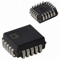
IC MIXER DWNCONV LOW DIST 20PLCC
Manufacturer
Analog Devices Inc
Series
AD831r
Specifications of AD831APZ
Rf Type
HF, VHF
Frequency
500MHz
Number Of Mixers
1
Gain
0dB
Noise Figure
14dB
Secondary Attributes
Down Converter
Current - Supply
125mA
Voltage - Supply
4.5 V ~ 5.5 V
Package / Case
20-LCC (J-Lead)
Supply Voltage Range
± 4.5V To ± 5.5V
Rf Ic Case Style
PLCC
No. Of Pins
20
Operating Temperature Range
-40°C To +85°C
Msl
MSL 1 - Unlimited
Termination Type
SMD
Operating Temperature (min)
-40C
Operating Temperature (max)
85C
Operating Temperature Classification
Industrial
Filter Terminals
SMD
Rohs Compliant
Yes
Lead Free Status / RoHS Status
Lead free / RoHS Compliant
Lead Free Status / RoHS Status
Lead free / RoHS Compliant, Lead free / RoHS Compliant
Available stocks
Company
Part Number
Manufacturer
Quantity
Price

Part Number:
AD831APZ
Manufacturer:
ADI/亚德诺
Quantity:
20 000
Company:
Part Number:
AD831APZ-REEL
Manufacturer:
PHI
Quantity:
2 000


THEORY OF OPERATION
The AD831 consists of a mixer core, a limiting amplifier, a low
noise output amplifier, and a bias circuit (Figure 1).
The mixer’s RF input is converted into differential currents by
a highly linear, Class A voltage-to-current converter, formed by
transistors Q1, Q2 and resistors R1, R2. The resulting currents
drive the differential pairs Q3, Q4 and Q5, Q6. The LO input is
through a high gain, low noise limiting amplifier that converts the
–10 dBm LO input into a square wave. This square wave drives
the differential pairs Q3, Q4 and Q5, Q6 and produces a high
level output at IFP and IFN—consisting of the sum and differ-
ence frequencies of the RF and LO inputs—and a series of lower
level outputs caused by odd harmonics of the LO frequency mix-
ing with the RF input.
An on-chip network supplies the bias current to the RF and LO
inputs when these are ac-coupled; this network is disabled when
the AD831 is dc-coupled.
REV. C
����������
�����
�����
�����
��
����
���
���
���
���
��
��
��
��
�
�
���������
��������
�������
����
��
��
��
��
���
��
���
Figure 1. Simplified Schematic Diagram
��������
��������
��
���
��
��
���
��
���
��
���
��
��
��
��
�
�
��
��������
���
��
–7–
���
���
When the integral output amplifier is used, pins IFN and IFP
are connected directly to pins AFN and AFP; the on-chip load
resistors convert the output current into a voltage that drives
the output amplifier. The ratio of these load resistors to resistors
R1, R2 provides nominal unity gain (0 dB) from RF-to-IF. The
expression for the gain, in decibels, is
where:
2
2
4
p
1
p
����
is the amplitude of the fundamental component of a
squarewave.
is the conversion loss.
is the small signal dc gain of the AD831 when the LO input
is driven fully positive or negative.
G
dB
�������
������
��������
=
���
���
��
�
20
log
���
���
10
Ê
Á
Ë
4
p
����
ˆ
˜
¯
���
Ê
Á
Ë
1
2
��������
ˆ
˜
¯
�
�
Ê
Á
Ë
p
2
���
ˆ
˜
¯
���
��
��
��
���
���
���
AD831
(1)
Related parts for AD831APZ
Image
Part Number
Description
Manufacturer
Datasheet
Request
R

Part Number:
Description:
MIXER IC
Manufacturer:
Analog Devices Inc
Datasheet:
Part Number:
Description:
MIXER IC
Manufacturer:
Analog Devices Inc
Datasheet:

Part Number:
Description:
±1.7g Dual-Axis IMEMS Accelerometer Evaluation Board
Manufacturer:
Analog Devices Inc
Datasheet:

Part Number:
Description:
Inertial Sensor Evaluation System
Manufacturer:
Analog Devices Inc
Datasheet:
Part Number:
Description:
Manufacturer:
Analog Devices Inc
Datasheet:
Part Number:
Description:
Manufacturer:
Analog Devices Inc
Datasheet:
Part Number:
Description:
Manufacturer:
Analog Devices Inc
Datasheet:
Part Number:
Description:
Manufacturer:
Analog Devices Inc
Datasheet:
Part Number:
Description:
Manufacturer:
Analog Devices Inc
Datasheet:
Part Number:
Description:
Manufacturer:
Analog Devices Inc
Datasheet:
Part Number:
Description:
Manufacturer:
Analog Devices Inc
Datasheet:
Part Number:
Description:
Manufacturer:
Analog Devices Inc
Datasheet: