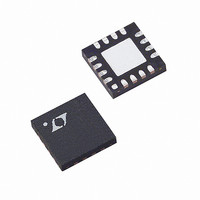
LT5512EUF Linear Technology, LT5512EUF Datasheet - Page 9

LT5512EUF
Manufacturer Part Number
LT5512EUF
Description
IC MIXER DWNCONV HI SIGN 16-QFN
Manufacturer
Linear Technology
Series
LT5512r
Datasheet
1.LT5512EUF.pdf
(12 pages)
Specifications of LT5512EUF
Rf Type
Cellular, HF, ISM, PCS, UHF, VHF, WMTS
Frequency
1kHz ~ 3GHz
Number Of Mixers
1
Gain
1.1dB
Noise Figure
14dB
Secondary Attributes
Down Converter
Current - Supply
74mA
Voltage - Supply
4.5 V ~ 5.25 V
Package / Case
16-WQFN Exposed Pad
Operating Temperature (min)
-40C
Operating Temperature (max)
85C
Operating Temperature Classification
Industrial
Lead Free Status / RoHS Status
Contains lead / RoHS non-compliant
Available stocks
Company
Part Number
Manufacturer
Quantity
Price
Part Number:
LT5512EUF
Manufacturer:
LINEAR/凌特
Quantity:
20 000
Part Number:
LT5512EUF#PBF
Manufacturer:
LINEAR/凌特
Quantity:
20 000
Company:
Part Number:
LT5512EUF#TRPBF
Manufacturer:
SP
Quantity:
5 997
Part Number:
LT5512EUF#TRPBF
Manufacturer:
LINEAR/凌特
Quantity:
20 000
APPLICATIO S I FOR ATIO
At high frequencies (greater than 900MHz), this same
matching technique is used, but it is important to consider
the IC’s input reactance when calculating the external induc-
tance. As shown in Figure 2, the high-frequency evaluation
board uses short (2mm) 72Ω microstrip lines to realize
the required inductance, instead of chip inductors.
External matching values for several frequencies, ranging
from 45MHz to 2.45GHz are shown in Figures 1 and 2.
Measured RF input return losses are plotted in Figure 5.
LO Input Port
The LO buffer amplifi er consists of high-speed limiting
differential amplifi ers, designed to drive the mixer quad
for high linearity. The LO
differential or single-ended drive. Both LO pins are inter-
nally biased to 2V
–5dBm
LO
IN
(140MHz, 450MHz, 900MHz and 1900MHz Matching)
0.01µF
0.01µF
Figure 6. LO Input with Resistive Matching
C6
C7
–10
–15
–20
–25
–30
–5
0
Figure 5. RF Input Return Loss
50
R1
100Ω
DC
U
100
.
140MHz
RF FREQUENCY (MHz)
+
U
15
14
and LO
LO
LO
450MHz
+
–
–
900MHz
pins are designed for
W
1000
1900MHz
V
CC
200Ω
5512 F05
3000
2V
U
200Ω
LT5512
5512 F06
Table 2. LO Input Differential Impedance
A simplifi ed schematic of the LO input is shown in Figure
6 with simple resistive matching and DC blocking capaci-
tors. This is the preferred matching for LO frequencies
below 1.5GHz. The internal (DC) resistance is 400Ω. The
required LO drive at the IC is 150mV
can come from a 50Ω source, or a higher impedance
source such as PECL. The external matching resistor is
required only to reduce the amplitude of the LO signal
at the IC, although the input stage will tolerate 10dB of
overdrive without signifi cant performance degradation.
Resistive LO port matching is used on the low-frequency
evaluation board (see Figure 1).
Above 1.5GHz, the internal capacitance becomes signifi cant
and reactive matching to 50Ω with a single series induc-
tor and DC blocking capacitors is preferred. A schematic
is shown in Figure 7. Table 2 lists the differential input
–10dBm
LO
50Ω
Frequency
IN
(MHz)
1000
1250
1500
1750
2000
2250
2500
2750
750
Figure 7. LO Input with Reactive Matching
100pF
C6
100pF
C7
L3
Differential Input
Impedance
263 + j172
213 + j178
175 + j173
146 + j164
125 + j153
108 + j142
95 + j131
86 + j122
78 + j133
15
14
LO
LO
+
–
V
CC
RMS
200Ω
0.766
0.760
0.752
0.743
0.733
0.722
0.709
0.695
Mag
0.68
Differential S11
(typical) which
2V
LT5512
200Ω
LT5512
Angle
–10.2
–13.4
–16.6
–19.8
–22.8
–25.8
–28.9
–31.8
–34.6
5512 F07
5512fa
9


