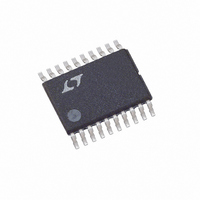
LT5503EFE Linear Technology, LT5503EFE Datasheet - Page 16

LT5503EFE
Manufacturer Part Number
LT5503EFE
Description
IC DIRECT IQ MOD/MIXER 20-TSSOP
Manufacturer
Linear Technology
Datasheet
1.LT5503EFE.pdf
(20 pages)
Specifications of LT5503EFE
Function
Modulator/Mixer
Lo Frequency
1.4GHz ~ 2.4GHz
Rf Frequency
1.7GHz ~ 2.7GHz
P1db
-15dBm
Noise Floor
-152dBm/Hz
Output Power
12.7dBm
Current - Supply
38mA
Voltage - Supply
1.8 V ~ 5.25 V
Test Frequency
2.4GHz
Package / Case
20-TSSOP Exposed Pad, 20-eTSSOP, 20-HTSSOP
Lead Free Status / RoHS Status
Contains lead / RoHS non-compliant
Available stocks
Company
Part Number
Manufacturer
Quantity
Price
Part Number:
LT5503EFE
Manufacturer:
LINEAR/凌特
Quantity:
20 000
Company:
Part Number:
LT5503EFE#PBF
Manufacturer:
LT
Quantity:
1 600
Part Number:
LT5503EFE#PBF
Manufacturer:
LINEAR/凌特
Quantity:
20 000
Part Number:
LT5503EFE#TRPBF
Manufacturer:
LINEAR/凌特
Quantity:
20 000
APPLICATIO S I FOR ATIO
LT5503
EVALUATION BOARD
Figure 6 shows the circuit schematic of the evaluation
board. The MODRFIN, MODRFOUT and MIXRFOUT ports
are matched to 50Ω at 2.45GHz. The LO1IN port is
matched to 50Ω at 2.1GHz and the LO2IN port is internally
matched.
A 390Ω resistor is used to reduce the quality factor (Q) of
the modulator output and deliver an output power of
–3dBm typically. A lower value resistor may be used if the
desired output power is lower. For example, the output
power will be 3dB lower if a 200Ω resistor is used.
Inductors with high self-resonance frequency should be
used for L1 to L6.
For simpler evaluation in a lab environment, the evaluation
board includes op amps to convert single-ended I and Q
input signals to differential . The op amp configuration has
a voltage gain of two; therefore the peak baseband input
voltage should be halved to maintain the same RF output
power. The op amp configuration shown will maintain
acceptable differential balance up to 10MHz typically. It is
also possible to bypass the op amps and drive the
modulator’s differential inputs directly by connecting to
the four oversized vias on the board (V1, V2, V3 and V4).
Figure 6 also shows a table of matching network values for
designs centered at 1.9GHz and1.2GHz.
Figure 7 shows the evaluation board with connectors and
ICs. Figure 8 shows the test set-up with the upconverting
mixer and IQ modulator connected in a transmit configu-
ration. Refer to the demo board DC365A Quick Start Guide
for detailed testing information.
16
U
U
W
U
RF Layout Tips:
• Use 50Ω impedance transmission lines up to the
• Keep the matching networks as close to the pins as
• Surface mount 0402 outline (or smaller) parts are
• Isolate the MODOUT pin from the LO2 input by putting
• The only ground connection is through the exposed pad
• Low impedance RF ground connections are essential
• V
• Separate power supply lines should be used to isolate
• Avoid use of long traces whenever possible. Long RF
matching networks, use of a ground plane is a must.
possible.
recommended to minimize parasitic inductances and
capacitances.
the LO2 transmission line on the bottom side of the
board.
on the bottom of the package. This exposed pad must
be soldered to the board in such a way to get complete
RF contact.
and can only be obtained by one or more vias tying
directly into the ground plane.
broadband capacitors to prevent instability.
the MODIN signal and other stray signals from the
MODOUT line. If possible, power planes should be
used.
traces in particular can lead to signal radiation and
degraded isolation, as well as higher losses.
CC
lines must be decoupled with low impedance,
5503f


