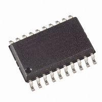
T5743P3-TGQ Atmel, T5743P3-TGQ Datasheet - Page 19

T5743P3-TGQ
Manufacturer Part Number
T5743P3-TGQ
Description
IC RCVR ASK/FSK 300MHZ 20-SOIC
Manufacturer
Atmel
Datasheet
1.T5743P6-TGQ.pdf
(41 pages)
Specifications of T5743P3-TGQ
Frequency
300MHz ~ 450MHz
Sensitivity
-108dBm
Data Rate - Maximum
10 kBaud
Modulation Or Protocol
ASK, FSK
Applications
General Purpose Data Transmission Systems
Current - Receiving
30mA
Data Interface
PCB, Surface Mount
Antenna Connector
PCB, Surface Mount
Voltage - Supply
4.5 V ~ 5.5 V
Operating Temperature
-40°C ~ 105°C
Package / Case
20-SOIC (0.300", 7.50mm Width)
Lead Free Status / RoHS Status
Contains lead / RoHS non-compliant
Features
-
Memory Size
-
Other names
T5743P3-TGQTR
Available stocks
Company
Part Number
Manufacturer
Quantity
Price
Company:
Part Number:
T5743P3-TGQ
Manufacturer:
PH
Quantity:
3 892
Figure 22. Timing Diagram of the Data Clock
Figure 23. Data Clock Disappears Because of a Timing Error
4569A–RKE–12/02
Dem_out
Data_out (DATA)
DATA_CLK
DATA_CLK
Dem_out
Data_out (DATA)
The data clock is available, after the data clock control logic has detected the distance
2T (Start bit) and is issued with the delay t
22).
If the data clock control logic detects a timing or logical error (Manchester code viola-
tion), like illustrated in Figure 23 and Figure 24, it stops the output of the data clock. The
receiver remains in receiving mode and starts with the bit check. If the bit check was
successful and the start bit has been detected, the data clock control logic starts again
with the generation of the data clock (see Figure 25).
It is recommended to use the function of the data clock only in conjunction with the bit
check 3, 6 or 9. If the bit check is set to 0 or the receiver is set to receiving mode via the
Pin POLLING/_ON, the data clock is available if the data clock control logic has
detected the distance 2T (Start bit).
Note that for Bi-phase-coded signals, the data clock is issued at the end of the bit.
'1'
'1'
Receiving mode,
data clock control
logic active
Bit check ok
Bit-check mode
Timing error
'1'
'1'
'1'
'1'
(T
T
ee
ee
Preburst
< T
'1'
'1'
Lim_min
OR T
T
'1'
Lim_max
'1'
2T
<T
Start bit
ee
Data
'0'
< T
'0'
Lim_min_2T
Receiving mode,
bit check active
data clock control logic active
'1'
'1'
OR T
Delay
Receiving mode,
ee
> T
'1'
'1'
Lim_max_2T
after the edge on Pin DATA (see figure
t
Delay
)
Data
'0'
'0'
'1'
'1'
t
P_Data_Clk
'0'
'0'
T5743
19


