MC33594FTAR2 Freescale Semiconductor, MC33594FTAR2 Datasheet - Page 11
MC33594FTAR2
Manufacturer Part Number
MC33594FTAR2
Description
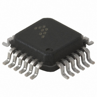
IC RF RECEIVER 315,434MHZ 24LQFP
Manufacturer
Freescale Semiconductor
Datasheet
1.MC33594FTAR2.pdf
(28 pages)
Specifications of MC33594FTAR2
Frequency
315MHz, 434MHz
Sensitivity
-105dBm
Data Rate - Maximum
11 kBaud
Modulation Or Protocol
FSK, OOK
Applications
General Data Transfer
Current - Receiving
5.7mA
Data Interface
PCB, Surface Mount
Antenna Connector
PCB, Surface Mount
Voltage - Supply
4.5 V ~ 5.5 V
Operating Temperature
-40°C ~ 105°C
Package / Case
24-LQFP
Operating Band Frequency
315 to 434MHz
Operating Frequency (max)
434000kHz
Operating Temperature (min)
-40C
Operating Temperature (max)
105C
Operating Temperature Classification
Industrial
Modulation Type
FSK/OOK
Package Type
LQFP
Product Depth (mm)
4mm
Product Length (mm)
4mm
Operating Supply Voltage (min)
4.5V
Operating Supply Voltage (typ)
5V
Operating Supply Voltage (max)
5.5V
Lead Free Status / RoHS Status
Contains lead / RoHS non-compliant
Features
-
Memory Size
-
Lead Free Status / Rohs Status
Compliant
Other names
MC33594FTAR2TR
Available stocks
Company
Part Number
Manufacturer
Quantity
Price


CONFIGURATION REGISTERS
Run time=T
© Motorola, Inc., 2002.
Table 4 describes the Configuration Register 1 (CR1).
Whatever SOE value has been programmed, a high level on STROBE sets the circuit into run mode.
Data are output on MOSI and the associated clock on SCLK.
Configuration Register 2 (CR2) defines the Identifier (ID) word content. The bits will be Manchester coded.
Table 8 describes the Configuration Register 3 (CR3).
- R/W controls the 3 registers access (read or write):
- CF defines the Carrier Frequency as shown onTable 5.
- MOD sets the data Modulation type:
- SOE enables the Strobe Oscillator:
- SR0/SR1 define the Strobe Ratio (SR) as shown on Table 6. SR is the ratio Sleep time over Run time and
- DME enables the Data Manager:
- HE defines if a Header word is present (the bit HE is only active if DME=1):
Strobe
0 = Write CR1, CR2 ,CR3,
1 = Read CR1, CR2, CR3.
0 = On/Off Keying (OOK) modulation,
1 = Frequency Shift Keying (FSK) modulation.
0 = Disabled,
1 = Enabled,
0 = Disabled,
1 = Enabled (to be combined with MOD=1).
0 = No header,
1 = Header.
Reset value
Reset value
Reset value
(where T
Bit name
Bit name
Bit name
Strobe
Freescale Semiconductor, Inc.
is the Strobe oscillator period).
R/W
DR1
bit 7
bit 7
bit 7
ID7
For More Information On This Product,
1
0
1
MOTOROLA SEMICONDUCTORS PRODUCTS
Table 5: Carrier Frequency selection
SR1
Table 4: Configuration Register 1
Table 7: Configuration Register 2
Table 8: Configuration Register 3
0
0
1
1
Table 6: Strobe Ratio selection
CF
0
1
DR0
bit 6
bit 6
bit 6
ID6
CF
Go to: www.freescale.com
1
0
0
SR0
0
1
0
1
Selected Frequency
MOD
MC33594
bit 5
bit 5
bit 5
ID5
MG
0
0
0
315MHz
434MHz
11
Strobe Ratio
SOE
bit 4
bit 4
bit 4
ID4
MS
1
0
0
15
31
3
7
bit 3
SR1
bit 3
bit 3
ID3
PG
0
0
0
bit 2
SR0
bit 2
bit 2
ID2
1
0
0
-
DME
bit 1
bit 1
bit 1
ID1
0
0
0
-
revision 1.1, 5 February 2002
bit 0
bit 0
bit 0
ID0
HE
0
0
0
-
Related parts for MC33594FTAR2
Image
Part Number
Description
Manufacturer
Datasheet
Request
R

Part Number:
Description:
Manufacturer:
Freescale Semiconductor, Inc
Datasheet:
Part Number:
Description:
Manufacturer:
Freescale Semiconductor, Inc
Datasheet:
Part Number:
Description:
Manufacturer:
Freescale Semiconductor, Inc
Datasheet:
Part Number:
Description:
Manufacturer:
Freescale Semiconductor, Inc
Datasheet:
Part Number:
Description:
Manufacturer:
Freescale Semiconductor, Inc
Datasheet:
Part Number:
Description:
Manufacturer:
Freescale Semiconductor, Inc
Datasheet:
Part Number:
Description:
Manufacturer:
Freescale Semiconductor, Inc
Datasheet:
Part Number:
Description:
Manufacturer:
Freescale Semiconductor, Inc
Datasheet:
Part Number:
Description:
Manufacturer:
Freescale Semiconductor, Inc
Datasheet:
Part Number:
Description:
Manufacturer:
Freescale Semiconductor, Inc
Datasheet:
Part Number:
Description:
Manufacturer:
Freescale Semiconductor, Inc
Datasheet:
Part Number:
Description:
Manufacturer:
Freescale Semiconductor, Inc
Datasheet:
Part Number:
Description:
Manufacturer:
Freescale Semiconductor, Inc
Datasheet:
Part Number:
Description:
Manufacturer:
Freescale Semiconductor, Inc
Datasheet:
Part Number:
Description:
Manufacturer:
Freescale Semiconductor, Inc
Datasheet: