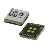
J3,0000,00,3.5 Navman Wireless, J3,0000,00,3.5 Datasheet - Page 14
J3,0000,00,3.5
Manufacturer Part Number
J3,0000,00,3.5
Description
MODULE GPS RECEIVER JUPITER 3
Manufacturer
Navman Wireless
Specifications of J3,0000,00,3.5
Frequency
1.575GHz
Sensitivity
-159dBm
Data Rate - Maximum
38.4kbps
Modulation Or Protocol
GPS
Applications
GPS
Current - Receiving
34mA
Data Interface
PCB, Surface Mount
Antenna Connector
PCB, Surface Mount
Voltage - Supply
2.7 V ~ 3 V
Operating Temperature
-40°C ~ 85°C
Package / Case
Module
Lead Free Status / RoHS Status
Lead free / RoHS Compliant
Features
-
Memory Size
-
Other names
943-1010-1


Jupiter
5.2.2 I/O surface mount pads
Details of the LGA pad functions are shown in Table 12.
NOTE: Follow design guidelines detailed in the Jupiter
NOTE: GPIO/RX-TX voltages and levels affected by supply voltage.
Pad No. Pad Names
3
10
11
12
13
14
15
16
17
18
19
20
21
22
23
24
25
26
27
28
29
30
31
32
1
2
3
4
5
6
7
8
9
|
Datasheet
RXB
TXB
TXA
RXA
ANT_CTRL
TIME_MARK
WTICK
ANT_SC
SPI_CS
GND
RF_IN
GND
RFPWRUP
VCC_RF
ANT_OC
GND
BOOT
GPIO2
GPS_FIX
SI
SO
GND
SPI_CLCK
VDD_RTC
RTC_XI
RTC_XO
nSRESET
VDD_BB
ON-OFF
nWAKEUP
FWD/REV
GND
Navman Wireless OEM Solutions • 27171 Burbank -Suite 200; Foothill Ranch, CA 92610-2501
TEL: +(949) 461-7150 • FAX: +(949) 461-7860 • www.navmanwirelessoem.com
Type
PWR
PWR
PWR
PWR
PWR
I/O
O
O
O
O
O
O
O
O
O
O
O
I
I
I
I
I
I
I
I
I
I
I
I
I
I
I
Table 12: I/O surface mount pads
Description
Serial Port B Receive - CMOS - levels affected by supply voltage
Serial Port B Transmit - CMOS - levels affected by supply voltage
Serial Port A Transmit - CMOS - levels affected by supply voltage
Serial Port A Receive - CMOS - levels affected by supply voltage
External Active antenna power control - Active High
DR version Wheel tick input
External Active antenna Short Circuit detect sense line - Active Low
SPI Chip select for DR version.
RF Ground
GPS signal input
RF Ground
RF Power enable - Active High
RF power input (2.7V to 3.0V)
External active antenna Open Circuit detect sense line - Active High
Power Ground
Boot pin for firmware update - Active High
General purpose I/O
GPS Fix Indication - Active Low
SPI IN - Connect to SO for GPS only firmware
SPI OUT - Connect to SI for GPS only firmware
Power Ground
DR version SPI CLOCK output.
RTC/BBRAM voltage input (1.1V to 1.3V)
RTC 32 KHz signal input - connect also to RTC crystal if no external
clock (2.8V SiGe input)
RTC 32 KHz signal output - connect only to RTC crystal
System Reset input - 200mSec low pulse as detailed
Digital and DSP power in (2.7V to 3.0V)
ON-OFF power control and PTF WAKEUP line
Digital and DSP power enable - Active Low.
DR version Forward/Reverse input
Power Ground
1PPS pulse
3
Integrator’s Manual.
12
Related parts for J3,0000,00,3.5
Image
Part Number
Description
Manufacturer
Datasheet
Request
R

Part Number:
Description:
ANTENNA GPS ACTIVE 5M CABLE
Manufacturer:
Navman Wireless
Datasheet:

Part Number:
Description:
DEV KIT FOR JUPITER 32XLP
Manufacturer:
Navman Wireless
Datasheet:

Part Number:
Description:
DEV KIT FOR JUPITER 30XLP
Manufacturer:
Navman Wireless
Datasheet:

Part Number:
Description:
DEV KIT FOR JUPITER 3 AND J3-30
Manufacturer:
Navman Wireless
Datasheet:

Part Number:
Description:
TERMINAL MDT-860 MOBILE DATA
Manufacturer:
Navman Wireless
Datasheet:


Part Number:
Description:
MODULE GPS JUPITER 30XLP 20CH
Manufacturer:
Navman Wireless
Datasheet:

Part Number:
Description:
MODULE GPS JUPITER 32XLP 20CH
Manufacturer:
Navman Wireless
Datasheet:

Part Number:
Description:
MODULE GPS RECEIVER JUPITER 3-30
Manufacturer:
Navman Wireless
Datasheet:

Part Number:
Description:
MODULE JUPITER 31 GPS W/R/A OSX
Manufacturer:
Navman Wireless
Datasheet:

Part Number:
Description:
MODULE GPS RECEIVER JUPITER 2
Manufacturer:
Navman Wireless
Datasheet:

Part Number:
Description:
DEV KIT FOR MDT860
Manufacturer:
Navman Wireless
Datasheet:

Part Number:
Description:
EVAL KIT GPS JUPITER 2
Manufacturer:
Navman Wireless
Datasheet: