RXM-869-ES_ Linx Technologies Inc, RXM-869-ES_ Datasheet - Page 2
RXM-869-ES_
Manufacturer Part Number
RXM-869-ES_
Description
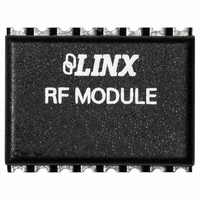
RECEIVER RF 869MHZ 16PIN SMD
Manufacturer
Linx Technologies Inc
Series
-r
Specifications of RXM-869-ES_
Frequency
869MHz
Sensitivity
-102dBm
Data Rate - Maximum
56 kbps
Modulation Or Protocol
FM, FSK
Current - Receiving
6.5mA
Data Interface
PCB, Surface Mount
Antenna Connector
PCB, Surface Mount
Voltage - Supply
4.5 V ~ 5.5 V
Operating Temperature
0°C ~ 70°C
Package / Case
16-SMD
Board Size
20.6 mm x 16 mm x 3.2 mm
Minimum Operating Temperature
0 C
Supply Voltage (min)
4.5 V
Product
RF Modules
Maximum Frequency
869.85 MHz
Supply Voltage (max)
5.5 V
Maximum Operating Temperature
+ 70 C
Applications
-
Memory Size
-
Features
-
Lead Free Status / RoHS Status
Lead free / RoHS Compliant
Features
-
Applications
-
Memory Size
-
Lead Free Status / Rohs Status
Lead free / RoHS Compliant
Other names
RXM-869-ES
RXM-869-ES
RXM-869-ES
Available stocks
Company
Part Number
Manufacturer
Quantity
Price
Company:

Part Number:
RXM-869-ES_
Manufacturer:
LNX
Quantity:
25


Table 1: ES Series Transmitter Specifications
Notes
1. Center frequency measured while modulated with a 0-5V square wave.
2. Into a 50-ohm load.
3. LADJ open.
4. Maximum power when LADJ open, minimum power when LADJ grounded.
5. DATA pin modulated with a 0-5V square wave.
6. The audio bandwidth is wide to accommodate the needs of the data slicer.
7. Characterized, but not tested.
8. The ES is optimized for both 0-5V and 0-3V modulation when sending digital data.
9. Analog signals, including audio, should be AC-coupled.
10. Time to transmitter readiness from the application of power to V
11. Maximum time without a data transition.
Page 2
ELECTRICAL SPECIFICATIONS
Parameter
POWER SUPPLY
Operating Voltage
Supply Current
Power-Down Current
TRANSMIT SECTION
Transmit Frequency:
Center Frequency Accuracy
Output Power
Output Power Control Range
Harmonic Emissions
Frequency Deviation
Data Rate
Analog/Audio Bandwidth
Data Input:
Power-Down Input:
Analog Input
ANTENNA PORT
RF Output Impedance
TIMING
Transmitter Turn-On Time
Max. Time Between Transitions
ENVIRONMENTAL
Operating Temperature Range
TXM-916-ES
TXM-869-ES
TXM-916-ES
TXM-869-ES
Logic Low
Logic High
Logic Low
Logic High
*CAUTION*
This product incorporates numerous static-sensitive components.
Always wear an ESD wrist strap and observe proper ESD handling
procedures when working with this device. Failure to observe this
precaution may result in module damage or failure.
Designation
R
F
V
I
I
PDN
P
P
V
V
F
CC
DEV
OUT
–
–
–
–
–
–
–
–
–
–
–
–
CC
IH
C
O
H
IL
Min.
200
2.1
5.5
-60
0.0
3.0
0.0
1.5
0.0
0.1
-3
80
70
20
–
–
–
–
–
–
–
0
Typical
916.48
869.85
90.0
3.0
7.0
-55
0.5
CC
65
50
–
0
–
–
–
–
–
–
–
–
–
–
–
or PDN going high.
56,000
28,000
Max.
+60
130
130
V
+70
4.0
8.5
-47
0.4
5.2
0.7
5.0
1.5
5.0
+4
–
–
–
–
–
CC
Units
mSec
mSec
VDC
MHz
MHz
dBm
VDC
VDC
VDC
VDC
kHz
dBc
kHz
kHz
V
mA
bps
µA
dB
Hz
°
Ω
P-P
C
Notes
2,3,7
7,10
7,11
2,3
6,7
–
–
7
4
4
1
2
5
5
7
8
8
–
–
9
7
7
Figure 3: Level Adjust Attenuation
Figure 5: Tx Powerup to Valid Rx Analog
ABSOLUTE MAXIMUM RATINGS
PERFORMANCE DATA
TYPICAL PERFORMANCE GRAPHS
1
2
CH1 2.00V
40
35
30
25
20
15
-10
These performance parameters are
based on module operation at 25°C
from a 3.0VDC supply unless
otherwise noted. Figure 2 illustrates
the connections necessary for
testing
recommended all ground pins be
connected to the ground plane.
-8.0
Supply voltage V
Any Input or Output Pin
Operating Temperature
Storage Temperature
Soldering Temperature
*NOTE*
damage to the device. Furthermore, extended operation at these maximum
ratings may reduce the life of this device.
CH2 500mV
Tx VCC/PDN
Rx Demodulated Analog Data
RF Output Attenuation (dB)
-6.0
and
-4.0
Exceeding any of the limits of this section may lead to permanent
100uS
operation.
-2.0
CC
-1.0
-0.4
It
-0.2
is
Figure 2: Test / Basic Application Circuit
Figure 4: Square-Wave Modulation Linearity
Figure 6: Tx Powerup to Valid Rx Data
1
2
1
2
-0.3
-0.5
-40
CH1 2.00V
CH1 1.66V
0
+216°C for 15 seconds
OUT
IN
RX Data
Tx VCC/PDN
1
2
3
4
5
CH2 2.00V
CH2 100mV
to
to V
to
to
PDN
LADJ
VCC
GND
DATA
CC
1mS
+4.0
+70
+90
LO_V_D
/CLK SE
250uS
+ 0.5
GND
/CLK
ANT
VDC
VDC
°C
°C
10
9
8
7
6
Page 3
Related parts for RXM-869-ES_
Image
Part Number
Description
Manufacturer
Datasheet
Request
R

Part Number:
Description:
RECEIVER 433MHZ LR SERIES
Manufacturer:
Linx Technologies Inc
Datasheet:

Part Number:
Description:
RECEIVER 418MHZ LR SERIES
Manufacturer:
Linx Technologies Inc
Datasheet:

Part Number:
Description:
RECEIVER 315MHZ LR SERIES
Manufacturer:
Linx Technologies Inc
Datasheet:

Part Number:
Description:
RECEIVER RF 916MHZ 16PIN SMD
Manufacturer:
Linx Technologies Inc
Datasheet:

Part Number:
Description:
RECEIVER RF 900MHZ 8-CH PACK
Manufacturer:
Linx Technologies Inc
Datasheet:

Part Number:
Description:
RECEIVER RF 900MHZ 8PAR/120SRLCH
Manufacturer:
Linx Technologies Inc
Datasheet:

Part Number:
Description:
MODULE USB LOW SPEED
Manufacturer:
Linx Technologies Inc
Datasheet:

Part Number:
Description:
IC TRANSCODER MT BI-DIR 20-SSOP
Manufacturer:
Linx Technologies Inc
Datasheet:

Part Number:
Description:
IC ENCODER LOW SECURITY 8DIP
Manufacturer:
Linx Technologies Inc
Datasheet:

Part Number:
Description:
IC DECODER MS SERIES 20-SSOP
Manufacturer:
Linx Technologies Inc
Datasheet:
Part Number:
Description:
IC ENCODER MS SERIES 20-SSOP
Manufacturer:
Linx Technologies Inc
Datasheet: