ATA8201-PXQW Atmel, ATA8201-PXQW Datasheet - Page 14

ATA8201-PXQW
Manufacturer Part Number
ATA8201-PXQW
Description
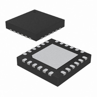
IC RCVR ASK/FSK UHF 315MHZ 24QFN
Manufacturer
Atmel
Datasheet
1.ATA8201-EK.pdf
(44 pages)
Specifications of ATA8201-PXQW
Frequency
315MHz
Sensitivity
-113dBm
Data Rate - Maximum
9.6 kbps
Modulation Or Protocol
ASK, FSK
Applications
AMR, ISM, Security and Access
Current - Receiving
6.7mA
Data Interface
PCB, Surface Mount
Antenna Connector
PCB, Surface Mount
Voltage - Supply
2.7 V ~ 3.3 V, 4.5 V ~ 5.5 V
Operating Temperature
-40°C ~ 85°C
Package / Case
24-VQFN Exposed Pad, 24-HVQFN, 24-SQFN, 24-DHVQFN
Lead Free Status / RoHS Status
Lead free / RoHS Compliant
Features
-
Memory Size
-
2.6
2.7
14
In-band Disturbers, Data Filter, Quasi-peak Detector, Data Slicer
RSSI Output
ATA8201/ATA8202
If a disturbing signal falls into the received band, or if a blocker is not a continuous wave, the
performance of a receiver strongly depends on the circuits after the IF filter. Hence, the demod-
ulator, data filter, and data slicer are important.
The data filter of the ATA8201/ATA8202 functions also as a quasi-peak detector. This results in a
good suppression of above mentioned disturbers and exhibits a good carrier-to-noise perfor-
mance. The required useful-signal-to-disturbing-signal ratio, at a BER of 10
in ASK mode and less than 3 dB (BR_Range_0 to BR_Range_2) and 6 dB (BR_Range_3) in
FSK mode. Due to the many different possible waveforms, these numbers are measured for the
signal, as well as for disturbers, with peak amplitude values. Note that these values are
worst-case values and are valid for any type of modulation and modulating frequency of the dis-
turbing signal, as well as for the receiving signal. For many combinations, lower
carrier-to-disturbing-signal ratios are needed.
The output voltage of the pin RSSI is an analog voltage, proportional to the input power level.
Using the RSSI output signal, the signal strength of different transmitters can be distinguished.
The usable dynamic range of the RSSI amplifier is 65 dB, the input power range P(RF
–110 dBm to –45 dBm, and the gain is 15 mV/dB.
typical device at 315 MHz with VS3V_AVCC = VS5V = 3V and T
input as shown in
needed for the same RSSI results.
Figure 2-9.
As can be seen in
and supply voltage range of ±3 dB. The total variance over production, temperature, and supply
voltage range is ±9 dB.
Typical RSSI Characteristic at 315 MHz Versus Temperature and Supply Voltage
Table 2-2
Figure 2-9 on page
0.4
1.6
1.4
1.3
1.2
0.7
0.5
1.7
1.5
1.0
0.9
0.8
0.6
1.1
-13 0 -12 0 -110 -10 0 -9 0
and
Figure 2-1 on page
max: +9 dBm
14, for single devices there is a variance over temperature
-8 0
Pin (dBm)
-70
min: -9 dBm
Figure 2-9
7. At 433.92 MHz, 1 dB more signal level is
-6 0
-50
-4 0
shows the RSSI characteristic of a
-3 0
3V, 25˚C
amb
-2 0
= 25°C with a matched
-10
–3,
is less than 14 dB
4971C–INDCO–04/09
IN
) is


