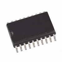
ATA5743P3-TKSY Atmel, ATA5743P3-TKSY Datasheet - Page 23

ATA5743P3-TKSY
Manufacturer Part Number
ATA5743P3-TKSY
Description
IC RCVR ASK/FSK 300KHZ 20SSOP
Manufacturer
Atmel
Datasheet
1.ATA5743P3-TGQY.pdf
(43 pages)
Specifications of ATA5743P3-TKSY
Frequency
300MHz ~ 450MHz
Sensitivity
-110dBm
Data Rate - Maximum
10 kBaud
Modulation Or Protocol
ASK, FSK
Applications
RKE, Telemetering, Security Technology
Current - Receiving
7.5mA
Data Interface
PCB, Surface Mount
Antenna Connector
PCB, Surface Mount
Voltage - Supply
4.5 V ~ 5.5 V
Operating Temperature
-40°C ~ 105°C
Package / Case
20-SOIC (0.200", 5.30mm Width)
Operating Frequency (max)
450000kHz
Operating Temperature (min)
-40C
Operating Temperature (max)
105C
Operating Temperature Classification
Industrial
Product Depth (mm)
4.4mm
Operating Supply Voltage (min)
4.5V
Operating Supply Voltage (typ)
5V
Operating Supply Voltage (max)
5.5V
Lead Free Status / RoHS Status
Lead free / RoHS Compliant
Features
-
Memory Size
-
Lead Free Status / Rohs Status
Compliant
Figure 6-20. Output of Digital Noise at the End of the Data Stream
Figure 6-21. Automatic Noise Suppression
Figure 6-22. Occurrence of a Pulse at the End of the Data Stream
6.5.2
4839B–RKE–08/05
Controlled Noise Suppression by the Microcontroller
Data_out (DATA)
DATA_CLK
DATA_CLK
Data_out (DATA)
Dem_out
Data_out (DATA)
DATA_CLK
Bit-check
mode
Bit-check
mode
Bit check ok
Bit check ok
The controlled noise suppressionis illustrated in
(see
of a valid data stream. To suppress the noise, the pin POLLING/_ON must be set to Low. The
receiver remains in receiving mode. Then, the OFF command causes the change to the start-up
mode. The programmed sleep time (see
level at pin POLLING/_ON is Low, but the bit check is active. The OFF command activates the
bit check also if the pin POLLING/_ON is held to Low. The receiver changes back to receiving
mode if the bit check was successful. To activate the polling mode at the end of the data trans-
mission, the pin POLLING/_ON must be set to High.
This way of suppressing the noise is recommended if the data stream is not Manchester or
Bi-phase coded.
Preburst
Preburst
Receiving mode,
data clock control
logic active
Table 6-9 on page
Receiving mode,
data clock control
logic active
Receiving mode,
data clock control
logic active
1
Data stream
Timing error
Data
Data
1
1
26) in the OPMODE register is set to “0”, digital noise appears at the end
Digital Noise
(
T
ee
T
Receiving mode,
bit check aktive
ee
< T
Lim_min
Bit-check
mode
or T
T
Digital Noise
Pulse
Lim_max
Table 6-7 on page
Bit check ok
Bit check ok
< T
Digital noise
Figure 6-23 on page
ee
Preburst
Preburst
Bit-check mode
< T
Receiving mode,
data clock control
logic active
Receiving mode,
data clock control
logic active
Lim_min_2T
26) will not be executed because the
Data
Data
or T
ee
> T
24. If the bit Noise_Disable
Lim_max_2T
Receiving mode,
bit check aktive
Digital Noise
Bit-check
mode
)
ATA5743
23


