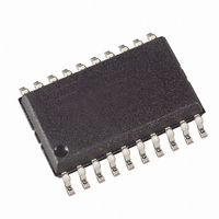
ATA3742P3-TGSY Atmel, ATA3742P3-TGSY Datasheet - Page 11

ATA3742P3-TGSY
Manufacturer Part Number
ATA3742P3-TGSY
Description
IC UHF ASK/FSK RECEIVER 20SOIC
Manufacturer
Atmel
Datasheet
1.ATA3742P3-TGQY.pdf
(34 pages)
Specifications of ATA3742P3-TGSY
Frequency
310MHz ~ 440MHz
Sensitivity
-108dBm
Data Rate - Maximum
10 kBaud
Modulation Or Protocol
ASK, FSK
Applications
RKE, TPM, Security Systems
Current - Receiving
7mA
Data Interface
PCB, Surface Mount
Antenna Connector
PCB, Surface Mount
Voltage - Supply
4.5 V ~ 5.5 V
Operating Temperature
-40°C ~ 105°C
Package / Case
20-SOIC (0.300", 7.50mm Width)
Operating Frequency (max)
450000kHz
Operating Temperature (min)
-40C
Operating Temperature (max)
105C
Operating Temperature Classification
Industrial
Operating Supply Voltage (min)
4.5V
Operating Supply Voltage (typ)
5V
Operating Supply Voltage (max)
5.5V
Lead Free Status / RoHS Status
Lead free / RoHS Compliant
Features
-
Memory Size
-
Lead Free Status / Rohs Status
Compliant
5. Polling Circuit and Control Logic
5.1
4900B–RKE–11/07
Basic Clock Cycle of the Digital Circuitry
The receiver is designed to consume less than 1 mA while being sensitive to signals from a cor-
responding transmitter. This is achieved via the polling circuit. This circuit enables the signal
path periodically for a short time. During this time, the bit check logic verifies the presence of a
valid transmitter signal. Only if a valid signal is detected does the receiver remain active and
transfer the data to the connected microcontroller. If there is no valid signal present, the receiver
is in sleep mode most of the time, resulting in low current consumption. This condition is called
polling mode. A connected microcontroller is disabled during that time.
All relevant parameters of the polling logic can be configured by the connected microcontroller.
This flexibility enables the user to meet the specifications in terms of current consumption, sys-
tem response time, data rate, etc.
Regarding the number of connection wires to the microcontroller, the receiver is very flexible. It
can be either operated by a single bi-directional line to save ports to the connected microcontrol-
ler, or it can be operated by up to three uni-directional ports.
The complete timing of the digital circuitry and the analog filtering is derived from one clock.
According to
(XTO) in combination with a divider. The division factor is controlled by the logical state at pin
MODE. As described in Section
(f
local oscillator (f
Figure 5-1.
Pin MODE can now be set in accordance with the desired clock cycle T
lowing application-relevant parameters:
XTO
• Timing of the polling circuit including bit check
• Timing of the analog and digital signal processing
• Timing of the register programming
• Frequency of the reset marker
• IF filter center frequency (f
) is defined by the RF input signal (f
Figure 5-1 on page
Generation of the Basic Clock Cycle
LO
).
IF0
Divider
)
“RF Front End” on page
:14/10
XTO
11, this clock cycle T
T
f
XTO
CLK
RFin
), which also defines the operating frequency of the
16
15
14
MODE
DVCC
XTO
L: USA (:10)
H: Europe (:14)
Clk
4, the frequency of the crystal oscillator
is derived from the crystal oscillator
Clk
. T
Clk
ATA3742
controls the fol-
11


