ENW-C9A08A3EF Panasonic - ECG, ENW-C9A08A3EF Datasheet - Page 15
ENW-C9A08A3EF
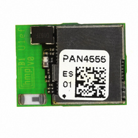
Manufacturer Part Number
ENW-C9A08A3EF
Description
MODULE ZIGBEE 2.4GHZ W/ANT
Manufacturer
Panasonic - ECG
Series
PAN4555r
Specifications of ENW-C9A08A3EF
Frequency
2.4GHz
Data Rate - Maximum
250kbps
Modulation Or Protocol
802.15.4 Zigbee
Applications
General Purpose
Power - Output
0dBm
Sensitivity
-87dBm
Voltage - Supply
2 V ~ 3.4 V
Current - Receiving
42mA
Current - Transmitting
35mA
Data Interface
PCB, Surface Mount
Memory Size
60kB Flash, 4kB RAM
Antenna Connector
On-Board, Chip
Operating Temperature
-40°C ~ 85°C
Package / Case
Module
Lead Free Status / RoHS Status
Lead free / RoHS Compliant
Other names
ENWC9A08A3EF
P13683TR
PAN4555-ANT
P13683TR
PAN4555-ANT


CLASSIFICATION
Einstufung
SUBJECT
Thema
CUSTOMER’S CODE
PAN4555
20. RECOMMENDED LAND PATTERN
HIGH FREQUENCY PRODUCTS DIVISION
Empfohlenes Land Pattern
Dimensions in mm.
The land pattern dimensions above can serve as a guidance, but this information is given
without any legal responsibility.
For your footprint, we recommend to use 50µm bigger size for the pads at each direction in
comparison to the module footprint, please refer to chapter 17. Foot Print of the Module.
For the solder paste screen please use the same as for the module, but slight different
measures and shapes of the solder paste screen cutouts might be optimum depending on your
soldering process, for example on the chosen solder paste screen thickness. The solder screen
thickness depends on your production standard, we recommend 120µm to 150µm.
IMPORTANT:
The bottom side of PAN4555 is fully coated, nevertheless no copper, such as through hole vias,
planes or tracks on your board component layer should be located below PAN4555 in order to
avoid short cuts. In cases where a track or through hole via has to be located under the module
it has to be kept away from PAN4555 bottom pads. The PN4555 multilayer pcb contains an
inner RF shielding plane, therefore no pcb shielding plane below the module is needed.
When using the antenna pad version and if your application allows, please place the antenna on
the edge of your carrier board.
PANASONIC ELECTRONIC DEVICES
When using the ceramic antenna,
means no ground, no line and in
In comparison to the module, we
this minimum area is restriced,
recommend to use 50 m bigger
general no metal, e.g. screws.
5.0 mm
pad size to each direction!
Module Business
EUROPE GmbH
MODEM FOR IEEE802.15.4 (ZIGBEE)
“ZigBee” Modem“ (IEEE802.15.4)
Antenna
PRODUCT SPECIFICATION
PANASONIC’S CODE
ENWC9A0xxxEF
Produktspezifikation
25
26
27
28
29
30
31
32
1
24
2
23
3
Pad 2 = 28 x 0.7mm x 1.4mm
Pad 1 = 4 x 1.1mm x 1.4mm
Top View
APPROVED
22
4
genehmigt
11.1 mm
21
5
20
6
19
7
18
No.
DS-4555-2400-102
PAGE
Seite
DATE
Datum
8
CHECKED
16
15
14
13
12
11
10
17
geprüft
9
14.02.2008
15 of 30
DESIGNED
erstellt
REV.
G
Related parts for ENW-C9A08A3EF
Image
Part Number
Description
Manufacturer
Datasheet
Request
R

Part Number:
Description:
MODULE BLUETOOTH SPP W/ANTENNA
Manufacturer:
Panasonic - ECG
Datasheet:

Part Number:
Description:
RF MODULE 802.15.4 W/ANT SNAP
Manufacturer:
Panasonic - ECG
Datasheet:
Part Number:
Description:
MOD BLUETOOTH PAN1321
Manufacturer:
Panasonic - ECG
Datasheet:

Part Number:
Description:
MOD BLUETOOTH HCI NO ANT PAN1315
Manufacturer:
Panasonic - ECG
Datasheet:

Part Number:
Description:
MODULE ZIGBEE 2.4GHZ W/SMD PADS
Manufacturer:
Panasonic - ECG
Datasheet:

Part Number:
Description:
MODULE ZIGBEE 2.4GHZ EMBER SMD
Manufacturer:
Panasonic - ECG
Datasheet:

Part Number:
Description:
MODULE ZIGBEE 2.4GHZ EMBER UFL
Manufacturer:
Panasonic - ECG
Datasheet:

Part Number:
Description:
MODULE ZIGBEE 2.4GHZ EMBER W/ANT
Manufacturer:
Panasonic - ECG
Datasheet:

Part Number:
Description:
RF MODULE 802.15.4 W/ANT SNAP
Manufacturer:
Panasonic - ECG
Datasheet:

Part Number:
Description:
RF MODULE 802.15.4 W/ANT SNAP
Manufacturer:
Panasonic - ECG
Datasheet:

Part Number:
Description:
MICROPHONE OMNI 6X2.2MM W/CAP
Manufacturer:
Panasonic - ECG
Datasheet:

Part Number:
Description:
CAP .01UF 100V PEN FILM 1210 5%
Manufacturer:
Panasonic - ECG
Datasheet:

Part Number:
Description:
FILTER LINE 23.3MH 2A
Manufacturer:
Panasonic - ECG
Datasheet:

Part Number:
Description:
SAW FILTER PCS 1960 MHZ 50/150
Manufacturer:
Panasonic - ECG
Datasheet: