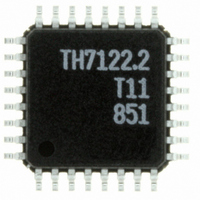
TH7122ENE Melexis Inc, TH7122ENE Datasheet - Page 15

TH7122ENE
Manufacturer Part Number
TH7122ENE
Description
IC TXRX 930MHZ FSK/FM/ASK 32LQFP
Manufacturer
Melexis Inc
Specifications of TH7122ENE
Frequency
300MHz ~ 930MHz
Data Rate - Maximum
115Kbps
Modulation Or Protocol
ASK, FM, FSK
Applications
Alarm and Security Systems, RKE, TPMS
Power - Output
-10dBm ~ 11dBm
Sensitivity
-105dBm
Voltage - Supply
2.2 V ~ 5.5 V
Current - Receiving
14mA
Current - Transmitting
23mA @ 10dBm
Data Interface
PCB, Surface Mount
Antenna Connector
PCB, Surface Mount
Operating Temperature
-40°C ~ 85°C
Package / Case
32-LQFP
Transmitting Current
12mA
Data Rate
115Kbps
Frequency Range
300MHz To 930MHz
Modulation Type
AM, FM, FSK
Sensitivity Dbm
-105dBm
Rf Ic Case Style
LQFP
No. Of Pins
32
Supply Voltage
RoHS Compliant
Output Power
10dBm
Rohs Compliant
Yes
Lead Free Status / RoHS Status
Lead free / RoHS Compliant
Memory Size
-
Lead Free Status / RoHS Status
Lead free / RoHS Compliant
Other names
TH7122.3
TH7122ENETR
TH7122ENETR
Available stocks
Company
Part Number
Manufacturer
Quantity
Price
3.2.5
The implemented FSK demodulator is based on the phase-coincidence principle. A discriminator tank, which
can either consist of a ceramic discriminator or an LC tank, is connected to pin IN_DEM. If FSK mode is
selected SW1 is open, SW2 is closed and the output of OA2 is multiplexed to pin INT2/PDO.
The demodulator output signal directly feeds the data slicer setup by means of OA1. The data slicer time
constant can be calculated using (8). This time constant should be larger than the longest possible bit dura-
tion of the data stream as described in the previous paragraph.
An on-chip AFC circuit tolerates input frequency variations. The input frequency acceptance range is propor-
tional to the FSK or FM deviation. It can be adjusted by the discriminator tank. The AFC feature is disabled
by default and can be activated in programmable mode.
3.3
The output of the PLL frequency synthesizer feeds a power amplifier (PA) in order to setup a complete RF
transmitter. The VCO frequency is identical to the carrier frequency.
3.3.1
The power amplifier (PA) has been designed to deliver about 10 dBm in the specified frequency bands. Its
pin OUT_PA is an open collector output. The larger the output voltage swing can be made the better the
power efficiency will be. The PA must be matched to deliver the best efficiency in terms of output power and
current consumption.
The collector must be biased to the positive supply. This is
done by means of an inductor parallel tuned with a capaci-
tor. Or it is made large enough in order not to affect the out-
put matching network. S-parameters of pin OUT_PA are not
useful because the output is very high resistive with a small
portion of parallel capacitance. Since the open-collector
output transistor can be considered as a current source, the
only parameters needed to design the output matching net-
work are the output capacitance, the supply voltage V
transistor’s saturation voltage and the power delivered to the
load P
In order to avoid saturation of the output stage, a saturation
voltage VCE
real part of the load impedance can then be calculated using
The output capacitance is typically 3 pF.
39010 07122
Rev. 010
O
Transmitter Part
.
FSK Demodulator
Power Amplifier
SAT
of about 0.7 V should be considered. The
R
L
=
(V
CC
−
2
VCE
⋅
P
Page 15 of 44
O
SAT
)
CC
2
, the
.
Fig. 7:
FSK/FM/ASK Transceiver
OUT_PA schematic
(9)
VCC
3pF
VEE
27 to 930MHz
TH7122
OUT_PA
L
Data Sheet
R
L
VCC
Feb/09


