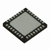
TRC105 RFM, TRC105 Datasheet - Page 43

TRC105
Manufacturer Part Number
TRC105
Description
IC TXRX 300MHZ-510MHZ 32TQFN
Manufacturer
RFM
Specifications of TRC105
Frequency
300MHz ~ 510MHz
Data Rate - Maximum
200kbps
Modulation Or Protocol
FSK, OOK
Applications
General Purpose
Power - Output
13dBm
Sensitivity
-112dBm
Voltage - Supply
2.1 V ~ 3.6 V
Current - Receiving
3mA
Current - Transmitting
30mA
Data Interface
PCB, Surface Mount
Antenna Connector
PCB, Surface Mount
Operating Temperature
-40°C ~ 85°C
Package / Case
32-TQFN
Wireless Frequency
300 MHz to 510 MHz
Output Power
13 dBm
Operating Supply Voltage
2.1 V to 3.6 V
Maximum Operating Temperature
+ 85 C
Mounting Style
SMD/SMT
Maximum Supply Current
1.7 mA
Minimum Operating Temperature
- 40 C
Modulation
FSK, OOK
Lead Free Status / RoHS Status
Lead free / RoHS Compliant
Memory Size
-
Lead Free Status / Rohs Status
Lead free / RoHS Compliant
Other names
583-1159-2
5.2 AC Electrical Characteristics
Minimum/maximum values are valid over the recommended operating range V
The electrical specifications given below are valid for a crystal having the specifications given in Table 3.
*Receiver in-circuit performance with RFM recommended SAW filter and crystal.
*Transmitter in-circuit performance with RFM recommended SAW filter and crystal.
www.RFM.com
©2009-2010 by RF Monolithics, Inc.
PARAMETER
RF Input Impedance
RF Input Power
Receiver Noise Figure
FSK Receiver Bandwidth
OOK Receiver Bandwidth
FSK Sensitivity, 2 kb/s*
10
F
FSK Sensitivity, 25 kb/s*
10
F
OOK Sensitivity, 2 kb/s*
10
Blocking Immunity*
Co-channel Rejection*
Adjacent Channel Rejection*
FSK Bit Rate
OOK Bit Rate
RSSI Resolution
RSSI Accuracy
RSSI Dynamic Range
Local Oscillator (LO) Emission
PARAMETER
RF Output Impedance
Maximum RF Output Power*
RF Output Power Range*
Spurious*
2
4
Phase Noise
FSK Deviation
nd
th
DEV
DEV
-3
-3
-3
and Higher Harmonics*
& 3
BER, BW = 100 kHz
BER, BW = 100 kHz
BER, BW = 50 kHz
= ±50 kHz
= ±50 kHz
rd
Harmonic*
E-mail:
info@rfm.com
SYM
SYM
MIN
1.56
1.56
MIN
±33
50
50
38
Technical support +1.800.704.6079
TYP
-110
-112
-110
-102
-104
-102
-108
-110
-108
TYP
-112
150
150
+13
±50
-12
0.5
-65
42
±3
63
70
21
53
8
TRANSMITTER
RECEIVER
Table 52
Table 53
MAX
MAX
±200
-110
-102
-108
-105
250
400
200
-46
-40
-40
32
0
DD
dBc/Hz
UNITS
UNITS
ohms
ohms
dBm
dBm
dBm
dBm
dBm
dBm
dBm
dBm
kb/s
kb/s
= 2.1-3.6V. Typical conditions: T
kHz
kHz
dBc
dBc
dBc
dBc
kHz
dB
dB
dB
dB
dB
signal strength of modulated co-channel signal
signal strength of unmodulated blocking signal
above 0 dBm receiver input may be damaged
signal strength of adjacent signal relative to
desired signal, 600 kHz offset, modulation
=> 150 kHz from carrier, no modulation,
relative to desired signal, 1 MHz offset
including SAW filter insertion loss
relative to desired signal
same as desired signal
Butterworth filter mode
polyphase filter mode
at maximum IF gain
at minimum IF gain
differential output
at 600 kHz offset
differential input
IC noise figure
programmable
programmable
no modulation
no modulation
300-330 MHz
470-510 MHz
300-330 MHz
470-510 MHz
300-330 MHz
470-510 MHz
Test Notes
Test Notes
434 MHz
434 MHz
434 MHz
NRZ
NRZ
o
= 25°C; V
TRC105 - 11/01/10
DD
= 3.3 V.
Page 43 of 66


