ATA5423-PLQW Atmel, ATA5423-PLQW Datasheet - Page 29
ATA5423-PLQW
Manufacturer Part Number
ATA5423-PLQW
Description
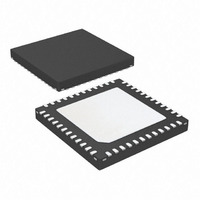
IC TXRX WIDEBAND 315MHZ 48QFN
Manufacturer
Atmel
Specifications of ATA5423-PLQW
Frequency
315MHz
Data Rate - Maximum
20kbps
Modulation Or Protocol
ASK, FSK
Applications
Alarm, ISM, Telemetry
Power - Output
5dBm
Sensitivity
-112.5dBm
Voltage - Supply
2.4 V ~ 3.6 V or 4.4 V ~ 6.6 V
Current - Receiving
10.5mA
Current - Transmitting
10mA
Data Interface
PCB, Surface Mount
Antenna Connector
PCB, Surface Mount
Operating Temperature
-40°C ~ 85°C
Package / Case
48-VQFN Exposed Pad, 48-HVQFN, 48-SQFN, 48-DHVQFN
Operating Temperature (min)
-40C
Operating Temperature (max)
85C
Operating Temperature Classification
Industrial
Product Depth (mm)
7mm
Product Height (mm)
0.9mm
Product Length (mm)
7mm
Lead Free Status / RoHS Status
Contains lead / RoHS non-compliant
Memory Size
-
Lead Free Status / Rohs Status
Compliant
Other names
ATA5423-PLQH
ATA5423-PLQHTR
ATA5423-PLQHTR
ATA5423-PLQWTR
ATA5423-PLQHTR
ATA5423-PLQHTR
ATA5423-PLQWTR


4.1
Figure 4-3.
4.2
4841D–WIRE–10/07
Pin CLK
Basic Clock Cycle of the Digital Circuitry
(Control register 3)
Clock Timing
N_RESET
CLK_ON
VSOUT
CLK
Pin CLK is an output to clock a connected microcontroller. The clock frequency f
as follows:
Because the enabling of pin CLK is asynchronous, the first clock cycle may be incomplete. The
signal at CLK output has a nominal 50% duty cycle.
The complete timing of the digital circuitry is derived from one clock. As shown in
on page
a divider.
T
The clock cycle of the bit check and the TX bit rate depends on the selected bit-rate range
(BR_Range) which is defined in control register 6 (see
is defined in control register 4 (see
the following formulas for further reference:
BR_Range
f
f
DCLK
DCLK
CLK
• Timing of the polling circuit including bit check
• TX bit rate
V
Thres_2
=
=
controls the following application relevant parameters:
f
---------- -
f
---------- -
XTO
27, this clock cycle T
= 2.38V (typically)
XTO
16
3
V
Thres_1
ATA5423/ATA5425/ATA5428/ATA5429
= 2.3V (typically)
DCLK
is derived from the crystal oscillator (XTO) in combination with
Table 7-13 on page
BR_Range 0: T
BR_Range 1: T
BR_Range 2: T
BR_Range 3: T
XDCLK
XDCLK
XDCLK
XDCLK
40). This clock cycle T
Table 7-20 on page
= 8
= 4
= 2
= 1
T
T
T
T
DCLK
DCLK
DCLK
DCLK
X
X
X
X
42) and XLim which
Lim
Lim
Lim
Lim
XDCLK
CLK
is defined by
is calculated
Figure 4-2
29
Related parts for ATA5423-PLQW
Image
Part Number
Description
Manufacturer
Datasheet
Request
R

Part Number:
Description:
IC TXRX ASK/FSK 315MHZ 48QFN
Manufacturer:
Atmel
Datasheet:


Part Number:
Description:
(ATA5423 - ATA5429) UHF ASK/FSK Transceiver
Manufacturer:
ATMEL Corporation
Datasheet:

Part Number:
Description:
DEV KIT FOR AVR/AVR32
Manufacturer:
Atmel
Datasheet:
Part Number:
Description:
INTERVAL AND WIPE/WASH WIPER CONTROL IC WITH DELAY
Manufacturer:
ATMEL Corporation
Datasheet:
Part Number:
Description:
Low-Voltage Voice-Switched IC for Hands-Free Operation
Manufacturer:
ATMEL Corporation
Datasheet:
Part Number:
Description:
MONOLITHIC INTEGRATED FEATUREPHONE CIRCUIT
Manufacturer:
ATMEL Corporation
Datasheet:
Part Number:
Description:
AM-FM Receiver IC U4255BM-M
Manufacturer:
ATMEL Corporation
Datasheet:
Part Number:
Description:
Monolithic Integrated Feature Phone Circuit
Manufacturer:
ATMEL Corporation
Datasheet:
Part Number:
Description:
Multistandard Video-IF and Quasi Parallel Sound Processing
Manufacturer:
ATMEL Corporation
Datasheet: