U3600BM-NFNY Atmel, U3600BM-NFNY Datasheet
U3600BM-NFNY
Specifications of U3600BM-NFNY


Related parts for U3600BM-NFNY


U3600BM-NFNY Summary of contents
Page 1
... RF parts such as IF converter, FM demodulator, RSSI, oscillators and PLL. Several gains and mutes in transmit and receive direction are controlled by the serial bus. The compander can be bypassed. Single-chip Cordless Telephone IC U3600BM Rev. 4516D–CT0–10/05 ...
Page 2
... GNDLO LO2 VCO3 :2 44 LO1 f LO sin cos 1 1 PCLO MixerT +45 -45 2 RFOGND 3 RFO VCO2 4 RFOVB 5 6 AGND VBIAS (1): PLL1: Modulator PLL U3600BM 2 MIX2O MIX2IN OSCGND XCK VAF MIX2GND Mixer2 Crystal Oscillator Serial Bus f Ref3 Bias (3) Phase Bat low Comparator Detector :D2 ...
Page 3
... VDD VSS DACO 30 15 OPOUT 29 16 OPIN 28 17 TXO 27 18 LIMIN 26 19 COUT 20 25 CTC 21 24 COIN 23 22 U3600BM LO1 LO2 GNDLO MIX1IN2 MIX1IN1 MIX1O OSCGND XCK VAF MIX2O MIX2GND MIX2IN IFIN1 IFIN2 ETC EXIN RECO1 RECO2 RXO DAIN MIC MICO 3 ...
Page 4
... MIX2O Mixer2 output 36 VAF Supply voltage for AF/IF parts 37 XCK Crystal oscillator input 11.15 MHz 38 OSCGND Oscillator ground 39 MIX1O Output of Mixer1 40 MIX1IN1 Symmetrical input of MIxer1 41 MIX1IN2 42 GNDLO Ground LO2 Tank elements for LO are connected to these pins 44 LO1 U3600BM 4 4516D–CT0–10/05 ...
Page 5
... In order to increase the adjustment range of VCO3 with fixed external tank elements and/or for “band switching”, especially for US frequencies, VCO3 has programmable capacitors inside. These capacitors can be added by serial bus (FA3 [4:0]) between LO1 and LO2. There are 31 steps available, every step adding a capacitor of 0.5 pF. 4516D–CT0–10/05 U3600BM 5 ...
Page 6
... In fact, the fractional divider divides Q during 223 cycles ----------------------------------------------------------------------------- - For each comparison cycle (f Q value and the divider divides by the P 1 exceeds 223, the divider divides by the value (P value (accumulator value - 223). After 223 cycles, the correct division is executed. U3600BM --------- - Mod 1 223 ...
Page 7
... Figure 3-1. Serial Bus Figure 3-2. Serial Bus Transmission Data D0 (D) Clock (C) Figure 3-3. Serial Bus Structure Data Clock 4516D–CT0–10/05 Data Micro- processor Clock 1st word Word transmission 4 0 Address Decoder 15 U3600BM 2nd word Transfer condition 8 128 Latches Commands 7 ...
Page 8
... MUXDA: DA(0:6): R1: Gain of earpeace amplifier and demodulator GEA4 GEA[0:4]: GDEM: R2: Switches and mutes for receive and data reception DATRX DATRX: BEXP: EEA: ERXO: ERX1: ERXHF: MRX: ERX2: U3600BM thd tch DA6 DA5 DA4 D/A multiplexing VBAT/RSSI Reference voltage D/A GEA3 GEA2 GEA1 Gain of earpeace amplifier ...
Page 9
... Enable the internal test mode mandatory that TM is kept to “0”! (if not 0, the circuit will not work as expected or described here in this paper) DR1I0 RA11 RA10 Rough adjustment VCO1 DV1F6 DV1F5 DV1F4 U3600BM free free MTX free free free KV21 M12 free ...
Page 10
... R13: VCO1 enable and fine adjustment EVCO1 EVCO1: SAFA1: EAFA1: FA1(0:4): R14: VCO2 enable and fine adjustment EVCO2 EVCO2: SAFA2: EAFA2: FA2(0:4): U3600BM 10 DV3I6 DV3I5 DV3I4 DV3I14 DV3I13 DV3I12 Fine adjustment VCO3 (frequency reduction) MSB FA32 FA31 FA30 Fine adjustment of VCO3 (frequency reduction); “0” is LSB, “4” is MSB ...
Page 11
... Selection phase comparator frequency for PLL3: f Selection phase comparator frequency for PLL3: f Symbol Batt amb T stg P tot Symbol R thJA U3600BM E12K5 E10K E6K25 = 25 kHz Ref3 = 12.5 kHz Ref3 = 10 kHz Ref3 = 6.25 kHz Ref3 = 5 kHz Ref3 = 2.5 kHz Ref3 Value 5.5 +125 – ...
Page 12
... Receiver Input Mixer (Mixer1), EVCO3 = EOSC = 1 Input frequency range Output frequency Input resistance MIX1IN1/MIX1IN2 to GND Input capacitance MIX1IN1/MIX1IN2 to GND Output impedance MIX1O MIX1IN1/2 -> MIX1O Voltage gain “Loaded” (330 “Unloaded” Input noise voltage U3600BM 12 Symbol with serial capacitance) Min. Typ. Max. Unit 3.1 3.6 5 µ ...
Page 13
... Gain adjust step Maximum gain load; increase input Output voltage swing voltage until distortion Input resistance 4516D–CT0–10/05 Symbol Min. 2.0 2.5 1200 –11 –21 –35 9 0.8 4.8 5% 7.3 U3600BM Typ. Max. Unit 140 100 mV 430 mV 3.0 4 3.5 pF 1500 1800 ...
Page 14
... Level Programming (Typical Values) RSSI level step size in the logarithmic region Table 6-1. RSSI Level Programming (Typical Values) Input Voltage VIF (µV) 0 25.4 42.4 424 4240 42400 U3600BM 14 Symbol Min. 1.6 0.5. 0.5. 0.35 RSSI Level (Decimal 111 Typ ...
Page 15
... U3600BM 18. Max. Unit 3 µA 50 4.1 V 3.35 V 5.25 V 4. MHz 2 µVrmsp 340 mVrms 11 ...
Page 16
... France: GMOD[1:0] = 01; fMod = 4.3 MHz GMOD[1:0] = 00; fMod = 4.3 MHz Spain/Netherlands: GMOD[1:0] = 10; fMod = 1.8 MHz Modulation frequency: 1 kHz Demodulated distortion THD US: MODIN - RFO France 2.5 kHz U3600BM 16 applied to LIMIN (AC coupled) RMS applied to LIMIN (AC coupled) RMS = 25°C j 20“ 4.0 kHz Figure 8-1 on page Symbol Min ...
Page 17
... Changing of oscillator frequency with FOSC reduction 4516D–CT0–10/05 Symbol Vil Vih Ii tsud thd tcl tch teon teh teoff Test Conditions/Pins FAOS (0: FAOS2 FAOS1 FAOS0 U3600BM Figure 8-1 on page 18. Min. Typ. Max –1 – 0.1 0.2 0.2 Min. Typ. Max. 11.15 + ...
Page 18
... Figure 8-1. Test Circuit TX-/Modulator- Loop Filter MODIN 5.6K 1U 100N DATA CLOCK DACO U3600BM 18 56K 24K PCLO LO1 RFOGND LO2 RFO GNDLO RFOVB MIX1IN2 AGND MIX1IN1 10N VBIAS MIX1O VRF VRF OSCGND MLF XCK LFGND VAF MODIN MIX2O VDD MIX2GND 470N ...
Page 19
... Figure 8-2. Application Circuit 4516D–CT0–10/05 Filter Duplex Antenna U3600BM 19 ...
Page 20
... Setting three integer divider in the mixer PLL and modulator PLL • Conversion gain adjustment of mixer PLL • Modulator gain • Setting of the pulling direction of PLL2 (value dependent frequency is higher or lower than LO frequency) • Demodulator gain Name Register Note: U3600BM 20 Function RA1[1:0] Rough adjust VCO1 RA2[1:0] Rough adjust VCO2 D1[1:0] ...
Page 21
... Mod and Q of fractional divider. The formulas take into account that the numerator of the M M /223 must not exceed 223 integer (Q M/223 223 integer (Q M/223 (Block Diagram),if M12 = (Block Diagram),if M12 = has to be reduced by a factor M. Simultaneously, Ref1 U3600BM and ...
Page 22
... France Modulation Loop Frequency and Divider f = 4.3 MHz 159 Mod M M U3600BM 22 D20 D3[1:0] KV2[3: 100 6.25 kHz Ref3 Rx Channel Frequency (MHz) 41.3125 41.3250 41.3375 41.3500 41.3625 41.3750 41.3875 41.4000 41.4125 41.4250 41 ...
Page 23
... 6.25 kHz Ref3 RX Channel Frequency (MHz) 26.3125 26.3250 26.3375 26.3500 26.3625 26.3750 26.3875 26.4000 26.4125 26.4250 26.4375 26.4500 26.4625 26.4750 26.4875 U3600BM GMOD[1:0] IMIXI DR1I[1:0] ( infra 1 VCO3 (MHz) 37.0125 37.0250 37.0375 37.0500 37.0625 37.0750 37.0875 37.1000 37.1125 37.1250 37.1375 37 ...
Page 24
... Spain Modulation Loop Frequency and Divider f = 557.5 kHz/ 1.8 MHz/4,P Ref1 Mod U3600BM 24 D20 D3[1:0] KV2[3: 001 6.25 kHz Ref3 RX Channel Frequency (MHz) 39.925 39.950 39.975 40.000 40.025 40.050 40.075 40.100 40.150 40 ...
Page 25
... 6.25 kHz Ref3 RX Channel Frequency (MHz) 31.025 31.050 31.075 31.100 31.125 31.150 31.175 31.200 31.250 31.275 31.300 31.325 = 12,Q = 204 U3600BM GMOD[1:0] IMIXI DR1I[1: high supra 1 VCO3 (MHz) 41.725 41.750 41.775 41.800 41.825 41.850 41.875 41.900 41.950 41.975 42.000 42 ...
Page 26
... Netherlands Modulation Loop Frequency and Divider f = 557.5 kHz/ 1.8 MHz/4,P Ref1 Mod U3600BM 26 D20 D3[1:0] KV2[3: 001 6.25 kHz Ref3 RX Channel Frequency (MHz) 39.9375 39.9625 39.9875 40.0125 40.0375 40.0625 40.0875 40.1125 40.1375 40 ...
Page 27
... 6.25 kHz Ref3 RX Channel Frequency (MHz) 31.0375 31.0625 31.0875 31.1125 31.1375 31.1625 31.1875 31.2125 31.2375 31.2625 31.2875 31.3125 = 12,Q = 204 U3600BM GMOD[1:0] IMIXI DR1I[1: high supra 1 VCO3 (MHz) 41.7375 41.7625 41.7875 41.8125 41.8375 41.8625 41.8875 41.9125 41.9375 41.9625 41.9875 42 ...
Page 28
... Table 10-19. Channel Frequencies and 1st LO Divider, f Channel TX Channel Frequency Number (MHz) 1 39.9375 2 39.9625 3 39.9875 4 40.0125 10.9.1 U.K. Modulation Loop Frequency and Divider f = 557.5 kHz/ 1.8 MHz/4,P Ref1 Mod U3600BM 28 D20 D3[1:0] KV2[3: 001 6.25 kHz Ref3 RX Channel Frequency (MHz) 39.9375 39.9625 39.9875 40.0125 = 12,Q ...
Page 29
... RX Channel Frequency (MHz) 48.760 48.840 48.860 48.920 49.020 49.080 49.100 49.160 49.200 49.240 49.280 49.360 49.400 49.460 49.500 U3600BM GMOD[1:0] IMIXI DR1I[1: low infra GMOD[1:0] IMIXI DR1I[1: infra 1 VCO3 (MHz) 38.970 39.145 39.160 39 ...
Page 30
... Number (MHz) 11 48.760 12 48.840 13 48.860 14 48.920 15 49.020 16 49.080 17 49.100 18 49.160 19 49.200 20 49.240 21 49.260 22 49.360 23 49.400 24 49.460 25 49.500 U3600BM 30 D20 D3[1:0] KV2[3: 100 D20 D3[1:0] KV2[3: 110 D2 = & kHz Ref3 RX Channel Frequency (MHz) 46.610 46.630 46.670 46.710 46.730 46.770 46.830 46.870 46.930 46 ...
Page 31
... 157 105 13 157 13 123 13 157 13 157 13 157 13 157 13 181 U3600BM f (MHz) Mod 7.640 7.485 7.510 7.640 7.555 7.640 7.640 7.640 7.640 7.700 f (MHz) Mod 5.66 5.60 5.66 5.62 5.60 5.58 5.72 5.70 5.68 5.66 5.74 5.70 5.70 5.70 5.68 31 ...
Page 32
... Portugal Modulation Loop Frequency and Divider f = 557.5 kHz/ 1.25 MHz/4,P Ref1 Mod U3600BM 32 D20 D3[1:0] KV2[3: 001 6.25 kHz Ref3 RX Channel Frequency (MHz) 37.000 37.025 37.050 37.075 37.100 37.125 37.150 37.175 37.200 37 ...
Page 33
... 6.25 kHz Ref3 RX Channel Frequency (MHz) 27.550 27.575 27.600 27.625 27.650 27.675 27.700 27.725 27.750 27.775 27.800 27.825 = 8,Q = 216 U3600BM GMOD[1:0] IMIXI DR1I[1: supra 1 VCO3 (MHz) 38.250 38.275 38.300 38.325 38.350 38.375 38.400 38.425 38.450 38.475 38.500 38.525 ...
Page 34
... Taiwan Modulation Loop Frequency and Divider f = 7.7 MHz 13,Q = 181 Mod M M U3600BM 34 D20 D3[1:0] KV2[3: 110 6.25 kHz Ref3 RX Channel Frequency (MHz) 48.2500 48.2750 48.3000 48.3250 48.3500 48.3750 48.4000 48.4250 48.4500 48 ...
Page 35
... D1[1:0] D20 D3[1:0] KV2[3: 110 6.25 kHz Ref3 RX Channel Frequency (MHz) 45.2500 45.2750 45.3000 45.3250 45.3500 45.3750 45.4000 45.4250 45.4500 45.4750 U3600BM GMOD[1:0] IMIXI DR1I[1: supra 1 VCO3 (MHz) 55.9500 55.9750 56.0000 56.0250 56.0500 56.0750 56.1000 56.1250 56.1500 56.1750 FRMT GDEM ...
Page 36
... China Modulation Loop Frequency and Divider f = 7.7 MHz 13,Q = 181 Mod M M U3600BM 36 D20 D3[1:0] KV2[3: 110 6.25 kHz Ref3 RX Channel Frequency (MHz) 48.0000 48.0250 48.0500 48.0750 48.1000 48.1250 48.1500 48.1750 48.2000 48 ...
Page 37
... Ref3 RX Channel Frequency (MHz) 45.0000 45.0250 450500 450750 45.1000 45.1250 45.1500 45.1750 45.2000 45.2250 45.2500 45.2750 45.3000 45.3250 45.3500 45.3750 45.4000 45.4250 45.4500 45.4750 U3600BM GMOD[1:0] IMIXI DR1I[1: supra 1 VCO3 (MHz) 55.7000 55.7250 55.7500 55.7750 55.8000 55.8250 55.8500 55.8750 55.9000 55.9250 55 ...
Page 38
... New Zealand Modulation Loop Frequency and Divider f = 4.7 MHz/ 8 Mod M M U3600BM 38 D20 D3[1:0] KV2[3: 110 6.25 kHz Ref3 RX Channel Frequency (MHz) 40.2500 40.2750 40.3000 40.3250 40.3500 40.3750 40.4000 40.4250 40.4500 40 ...
Page 39
... D1[1:0] D20 D3[1:0] KV2[3: 101 6.25 kHz Ref3 RX Channel Frequency (MHz) 34.2500 34.2750 34.3000 34.3250 34.3500 34.3750 34.4000 34.4250 34.4500 34.4750 U3600BM GMOD[1:0] IMIXI DR1I[1: supra 1 VCO3 (MHz) 44.9500 44.9750 45.0000 45.0250 45.0500 45.0750 45.1000 45.1250 45.1500 45.1750 FRMT GDEM ...
Page 40
... U3600BM 40 D20 D3[1:0] KV2[3: 100 kHz Ref3 RX Channel Frequency (MHz) 49.6700 49.8450 49.8600 49.7700 49.8750 49.8300 49.8900 49.9300 49.9900 49.9700 49.6950 49.7100 49.7250 49.7400 49.7550 GMOD[1:0] ...
Page 41
... kHz Ref3 RX Channel Frequency (MHz) 46.6100 46.6300 46.6700 46.7100 46.7300 46.7700 46.8300 46.8700 46.9300 46.9700 46.5100 46.5300 46.5500 46.5700 46.5900 U3600BM GMOD[1:0] IMIXI DR1I[1: supra 1 VCO3 (MHz) 57.3100 57.3300 57.3700 57.4100 57.4300 57.4700 57.5300 57.5700 57.6300 57.6700 57.2100 57.2300 57 ...
Page 42
... Table 10-51. Crystal Specifications Drive level < 0.01 µW Parameters Load resonance frequency with 14 pF load capacitance Load capacitance Frequency tolerance Shunt capacitance Motional capacitance Series resistance Note: (1) Necessary to stay within adjustment range of oscillator FAOS (0: ... 5 U3600BM 157 105 13 157 13 123 13 157 ...
Page 43
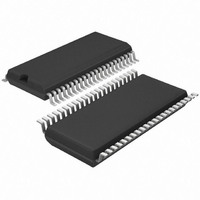
... Ordering Information Extended Type Number U3600BM-NFNY U3600BM-NFNG3Y 12. Package Information Package SSO44 Dimensions in mm 0.3 0 4516D–CT0–10/05 Package SSO44 SSO44 18.05 17.80 0.25 0.10 16 U3600BM Remarks Tube, Pb-free Taped and reeled, Pb-free 9.15 8.65 7.50 7.30 2.35 10.50 10.20 technical drawings ...
Page 44
... Disclaimer: The information in this document is provided in connection with Atmel products. No license, express or implied, by estoppel or otherwise, to any intellectual property right is granted by this document or in connection with the sale of Atmel products. EXCEPT AS SET FORTH IN ATMEL’S TERMS AND CONDI- TIONS OF SALE LOCATED ON ATMEL’S WEB SITE, ATMEL ASSUMES NO LIABILITY WHATSOEVER AND DISCLAIMS ANY EXPRESS, IMPLIED OR STATUTORY WARRANTY RELATING TO ITS PRODUCTS INCLUDING, BUT NOT LIMITED TO, THE IMPLIED WARRANTY OF MERCHANTABILITY, FITNESS FOR A PARTICULAR PURPOSE, OR NON-INFRINGEMENT ...