TR3005 RFM, TR3005 Datasheet - Page 9
TR3005
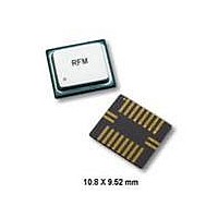
Manufacturer Part Number
TR3005
Description
ASH TR 115.2 KBPS 403.5 MHZ
Manufacturer
RFM
Series
TRr
Datasheet
1.TR3005.pdf
(12 pages)
Specifications of TR3005
Frequency
403.55MHz
Data Rate - Maximum
115.2kbps
Modulation Or Protocol
ASK, OOK
Applications
ISM
Power - Output
0dBm
Sensitivity
-109dBm
Voltage - Supply
2.2 V ~ 3.7 V
Current - Receiving
3.8mA
Current - Transmitting
7.5mA
Data Interface
PCB, Surface Mount
Antenna Connector
PCB, Surface Mount
Operating Temperature
-10°C ~ 55°C
Package / Case
SM-20H
Wireless Frequency
403.5 MHz
Operating Supply Voltage
2.5 V, 3.3 V
Maximum Operating Temperature
+ 85 C
Mounting Style
SMD/SMT
Maximum Data Rate
115.2 Kbps
Minimum Operating Temperature
- 10 C
Modulation
OOK/ASK
Lead Free Status / RoHS Status
Lead free by exemption / RoHS compliant by exemption
Memory Size
-
Lead Free Status / Rohs Status
Lead free / RoHS Compliant
Other names
583-1090-2


Pin De scrip tions
Pin
1
2
3
4
5
6
7
AGCCAP
RXDATA
BBOUT
PKDET
CMPIN
GND1
Name
VCC1
GND1 is the RF ground pin. GND2 and GND3 should be connected to GND1 by short, low-inductance traces.
VCC1 is the pos i tive sup ply volt age pin for the trans mit ter out put am pli fier and the re ceiver base-band cir cuitry.
VCC1 is usu ally con nected to the pos i tive sup ply through a fer rite RF de coup ling bead, which is by passed by an
RF ca pac i tor on the sup ply side. See the ASH Trans ceiver De signer’s Guide for ad di tional in for ma tion.
This pin con trols the AGC re set op er a tion. A ca pac i tor be tween this pin and ground sets the min i mum time the
AGC will hold-in once it is en gaged. The hold-in time is set to avoid AGC chat ter ing. For a given hold-in time t
the ca pac i tor value C
A ±10% ce ramic ca pac i tor should be used at this pin. The value of C
tween t
the AGC to ride through the lon gest run of zero bits that can oc cur in a re ceived data stream. The AGC hold-in
time can be greater than the peak de tec tor de cay time, as dis cussed be low. How ever, the AGC hold-in time
should not be set too long, or the re ceiver will be slow in re turn ing to full sen si tiv ity once the AGC is en gaged by
noise or in ter fer ence. The use of AGC is op tional when us ing OOK mod u la tion with data pulses of at least 30 µs.
AGC op er a tion can be de feated by con nect ing this pin to Vcc. Ac tive or latched AGC op er a tion is re quired for
ASK mod u la tion and/or for data pulses of less than 30 µs. The AGC can be latched on once en gaged by con nect -
ing a 150 K re sis tor be tween this pin and ground, in stead of a ca pac i tor. AGC op er a tion de pends on a func tion ing
peak de tec tor, as dis cussed be low. The AGC ca pac i tor is dis charged in the re ceiver power-down (sleep) mode
and in the trans mit modes.
This pin con trols the peak de tec tor op er a tion. A ca pac i tor be tween this pin and ground sets the peak de tec tor at -
tack and de cay times, which have a fixed 1:1000 ra tio. For most ap pli ca tions, these time con stants should be co -
or di nated with the base-band time con stant. For a given base-band ca pac i tor C
A ±10% ce ramic ca pac i tor should be used at this pin. This time con stant will vary be tween t
vari a tions in sup ply volt age, tem per a ture, etc. The ca pac i tor is driven from a 200 ohm “at tack” source, and de cays
through a 200 K load. The peak de tec tor is used to drive the “dB-below-peak” data slicer and the AGC re lease
func tion. The AGC hold-in time can be ex tended be yond the peak de tec tor de cay time with the AGC ca pac i tor, as
dis cussed above. Where low data rates and OOK mod u la tion are used, the “dB-below-peak” data slicer and the
AGC are op tional. In this case, the PKDET pin and the THLD2 pin can be left un con nected, and the AGC pin can
be con nected to Vcc to re duce the num ber of ex ter nal com po nents needed. The peak de tec tor ca pac i tor is dis -
charged in the re ceiver power-down (sleep) mode and in the trans mit modes.
BBOUT is the re ceiver base-band out put pin. This pin drives the CMPIN pin through a cou pling ca pac i tor C
in ter nal data slicer op er a tion. The time con stant t
A ±10% ce ramic ca pac i tor should be used be tween BBOUT and CMPIN. The time con stant can vary be tween t
and 1.8*t
stance will de pend on the data rate, data run length, and other fac tors as dis cussed in the ASH Trans ceiver De -
signer’s Guide. A com mon cri te ria is to set the time con stant for no more than a 20% volt age droop dur ing SP
For this case:
The out put from this pin can also be used to drive an ex ter nal data re cov ery pro cess (DSP, etc.). The nom i nal out -
put im ped ance of this pin is 1 K. When the re ceiver RF am pli fi ers are op er at ing at a 50%-50% duty cy cle, the
BBOUT sig nal changes about 10 mV/dB, with a peak-to-peak sig nal level of up to 685 mV. For lower duty cy cles,
the mV/dB slope and peak-to-peak sig nal level are pro por tion ately less. The sig nal at BBOUT is rid ing on a
1.1 Vdc value that var ies some what with sup ply volt age and tem per a ture, so it should be cou pled through a ca -
pac i tor to an ex ter nal load. A load im ped ance of 50 K to 500 K in par al lel with no more than 10 pF is rec om -
mended. When an ex ter nal data re cov ery pro cess is used with AGC, BBOUT must be cou pled to the ex ter nal
data re cov ery pro cess and CMPIN by sep a rate se ries cou pling ca pac i tors. The AGC re set func tion is driven by
the sig nal ap plied to CMPIN. When the trans ceiver is in power-down (sleep) or in a trans mit mode, the out put im -
ped ance of this pin be comes very high, pre serving the charge on the cou pling ca pac i tor.
This pin is the in put to the in ter nal data slic ers. It is driven from BBOUT through a cou pling ca pac i tor. The in put
im ped ance of this pin is 70 K to 100 K.
RXDATA is the re ceiver data out put pin. This pin will drive a 10 pF, 500 K par al lel load. The peak cur rent avail able
from this pin in creases with the re ceiver low-pass fil ter cut off fre quency. In the power-down (sleep) or trans mit
modes, this pin be comes high im ped ance. If re quired, a 1000 K pull-up or pull-down re sis tor can be used to es tab -
lish a def i nite logic state when this pin is high im ped ance. If a pull-up re sis tor is used, the pos i tive sup ply end
should be con nected to a volt age no greater than Vcc + 200 mV.
AGH
BBC
C
C
t
C
BBC
AGC
PKD
BBO
and 2.65* t
with vari a tions in sup ply volt age, tem per a ture, etc. The op ti mum time con stant in a given cir cum -
= 0.064*C
= 0.33* C
= 19.1* t
= 70*SP
AGC
AGH
MAX
AGH
BBO
BBO
is:
, de pend ing on op er at ing volt age, tem per a ture, etc. The hold-in time is cho sen to al low
, where SP
, where t
, where t
, where C
AGH
BBC
MAX
BBO
is in µs and C
is in µs and C
and C
is the max i mum sig nal pulse width in µs and C
9
PKD
BBC
Description
are in pF
AGC
for this con nec tion is:
BBO
is in pF
is in pF
AGC
given above pro vides a hold-in time be -
BBO
, the ca pac i tor value C
BBO
PKA
is in pF
and 1.5* t
PKA
PKD
BBO
with
is:
AGH
MAX
for
BBC
,
.
Related parts for TR3005
Image
Part Number
Description
Manufacturer
Datasheet
Request
R

Part Number:
Description:
TRANSCEIVER RF 916MHZ 1/2-DUPLEX
Manufacturer:
Linx Technologies Inc
Datasheet:
Part Number:
Description:
TRANSCEIVER RF 916MHZ 1/2-DUPLEX
Manufacturer:
Linx Technologies Inc
Datasheet:
Part Number:
Description:
TXCVR RF 900MHZ 1/2-DUPLEX 180CH
Manufacturer:
Linx Technologies Inc
Part Number:
Description:
TRANSCEIVER RF 916MHZ 20PIN SMD
Manufacturer:
Linx Technologies Inc
Datasheet:

Part Number:
Description:
ASH TR 115.2 KBPS 433.92 MHZ
Manufacturer:
RFM
Datasheet:

Part Number:
Description:
ASH TR 115.2 KBPS 916.5 MHZ
Manufacturer:
RFM
Datasheet:

Part Number:
Description:
ASH TR 115.2 KBPS 433.92 MHZ
Manufacturer:
RFM
Datasheet:
Part Number:
Description:
ASH TR 115.2 KBPS 916.5 MHZ
Manufacturer:
RFM
Datasheet:

Part Number:
Description:
ASH RX 115.2 KBPS 433.92 MHZ
Manufacturer:
RFM
Datasheet:

Part Number:
Description:
RFIC TRANCEIVER MULTI-CHANNEL FS
Manufacturer:
RFM
Datasheet:
Part Number:
Description:
10-Terminal Ceramic Surface-Mount Case 7 x 5 mm Nominal Footprint
Manufacturer:
RFM [RF Monolithics, Inc]
Datasheet:
Part Number:
Description:
QUAD-BAND GSM850/GSM/DCS/PCS POWER AMP MODULE
Manufacturer:
RFM [RF Monolithics, Inc]
Datasheet:
Part Number:
Description:
402 to 405 MHz Medical Band Front-end Filter
Manufacturer:
RFM [RF Monolithics, Inc]
Datasheet:
Part Number:
Description:
674.03 MHz SAW Resonator
Manufacturer:
RFM [RF Monolithics, Inc]
Datasheet: