DM1810-434MN RFM, DM1810-434MN Datasheet
DM1810-434MN
Specifications of DM1810-434MN


Related parts for DM1810-434MN


DM1810-434MN Summary of contents
Page 1
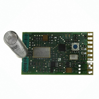
... The DM1810 family is designed for adding wireless mesh connectivity to a wide range of moni- toring and control systems. The DM1810-434MN is equipped with a serial I/O port to interface to a host microcontroller. The module also includes an analog input, a logic input, and a logic output for monitoring and control. Radio communications range in an “ ...
Page 2
... Regulated Power Supply Output Voltage, VIN 3 Regulated Power Supply Voltage Ripple Relative Humidity Range, Non-Condensing www.RFM.com E-mail: info@rfm.com ©2008 by RF Monolithics, Inc. Sym Notes VIN o C VIN VOUT RH Minimum Typical Maximum Units 1.1 mA 1.2 mA 1.2 9.6 kb/s 60 µA 3.1 10 2.6 10 3.0 Vdc Page DM1810-434MN - 4/17/ P-P ...
Page 3
... The 16F689 provides a 9.6 kb/s serial interface for communication with a host microcontroller. A compan- ion interface board, the IM1800, is also available with USB bridge circuitry to interface the DM1810-434MN to a host PC. Three of the 16F689 I/O pins are config- ured for external monitoring or control. Digital In is configured as a logic input with a weak pull-up for sensing a contact closure to a DM1810 ground pad ...
Page 4
... DM1810-434MN I/O Pad Descriptions Pin Name J1-1 GND This pad is a signal and power supply ground. J1-2 VIN This is the power supply input pad. The allowed input voltage range is 2 VOUT tracks 50 to 100 mV below VIN when VIN is in the range of 2.6 to 3.1 V. When VIN is in the range of 3 VOUT is regulated at 3 ...
Page 5
... Note: Specifications subject to change without notice. www.RFM.com E-mail: info@rfm.com ©2008 by RF Monolithics, Inc. Figure 2 Figure 3 Page DM1810-434MN - 4/17/08 ...