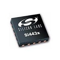
SI4431-B1-FM Silicon Laboratories Inc, SI4431-B1-FM Datasheet - Page 19

SI4431-B1-FM
Manufacturer Part Number
SI4431-B1-FM
Description
IC TXRX 240-930MHZ -8-13DB 20QFN
Manufacturer
Silicon Laboratories Inc
Specifications of SI4431-B1-FM
Package / Case
20-VQFN
Mfg Application Notes
Transitioning SI4430/31 to Rev B
Frequency
240MHz ~ 930MHz
Data Rate - Maximum
256kbps
Modulation Or Protocol
FSK, GFSK, OOK
Applications
General Purpose
Power - Output
13dBm
Sensitivity
-121dBm
Voltage - Supply
1.8 V ~ 3.6 V
Current - Receiving
18.5mA
Current - Transmitting
30mA
Data Interface
PCB, Surface Mount
Antenna Connector
PCB, Surface Mount
Operating Temperature
-40°C ~ 85°C
Wireless Frequency
240 MHz to 930 MHz
Output Power
13 dBm
Operating Supply Voltage
1.8 V to 3.6 V
Maximum Operating Temperature
+ 85 C
Mounting Style
SMD/SMT
Maximum Supply Current
30 mA
Minimum Operating Temperature
- 40 C
Modulation
FSK, GFSK, OOK
Operating Temperature (min)
-40C
Operating Temperature (max)
85C
Operating Temperature Classification
Industrial
Product Depth (mm)
4mm
Product Length (mm)
4mm
Operating Supply Voltage (min)
1.8V
Operating Supply Voltage (typ)
3V
Operating Supply Voltage (max)
3.6V
Lead Free Status / RoHS Status
Lead free / RoHS Compliant
Memory Size
-
Lead Free Status / Rohs Status
Lead free / RoHS Compliant
Available stocks
Company
Part Number
Manufacturer
Quantity
Price
Company:
Part Number:
SI4431-B1-FMR
Manufacturer:
TE
Quantity:
2 000
Part Number:
SI4431-B1-FMR
Manufacturer:
SILICON LABS/芯科
Quantity:
20 000
The SPI interface contains a burst read/write mode which allows for reading/writing sequential registers without
having to re-send the SPI address. When the nSEL bit is held low while continuing to send SCLK pulses, the SPI
interface will automatically increment the ADDR and read from/write to the next address. An example burst write
transaction is illustrated in Figure 5 and a burst read in Figure 6. As long as nSEL is held low, input data will be
latched into the Si4430/31/32 every eight SCLK cycles.
SDO
SCLK
nSEL
SCLK
nSEL
SDI
SDI
First Bit
First Bit
RW
RW
=1
=0
SDO
SCLK
nSEL
SDI
A6
A6
A5
A5
First Bit
A4
A4
RW
=0
A3
A3
A6
A2
A2
Figure 5. SPI Timing—Burst Write Mode
Figure 6. SPI Timing—Burst Read Mode
A5
Figure 4. SPI Timing—READ Mode
A1
A1
A4
First Bit
A0
A0
A3
D7
=X
D7
D7
=X
A2
D6 D5 D4 D3
D6
=X
D6
=X
A1
D5
=X
D5
=X
First Bit
A0
Rev 1.1
D4
=X
D4
=X
D7
D7
=X
D3
=X
D3
=X
D6 D5 D4 D3
D6
=X
D2
=X
D2
=X
D2 D1 D0
D5
=X
Last Bit
D1
=X
D1
=X
D4
=X
D0
=X
D0
=X
D3
=X
D7
=X
D7 D6 D5 D4 D3
D2
=X
D2 D1 D0
Si4430/31/32-B1
D6
=X
D1
=X
D5
=X
Last Bit
D0
=X
Last Bit
D4
=X
D3
=X
D2
=X
D2 D1 D0
D1
=X
Last Bit
D0
=X
19


