DM2200-916VM-1 RFM, DM2200-916VM-1 Datasheet - Page 3
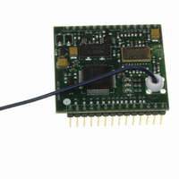
DM2200-916VM-1
Manufacturer Part Number
DM2200-916VM-1
Description
916.5 MHZ, 10 MW MESH MODULE, SE
Manufacturer
RFM
Series
DM2200r
Datasheet
1.DM2200-916VM-1.pdf
(6 pages)
Specifications of DM2200-916VM-1
Frequency
916.5MHz
Data Rate - Maximum
9.6kbps
Modulation Or Protocol
OOK
Applications
Wireless Mesh Networks
Power - Output
10dBm
Voltage - Supply
2.9 V ~ 3.6 V
Current - Receiving
6mA
Current - Transmitting
36mA
Data Interface
PCB, Through Hole
Antenna Connector
On-Board, Whip
Operating Temperature
-40°C ~ 85°C
Package / Case
Module
Lead Free Status / RoHS Status
Lead free / RoHS Compliant
Sensitivity
-
Memory Size
-
Lead Free Status / Rohs Status
Lead free / RoHS Compliant
Other names
583-1043


DM2200-916VM-1 FCC Certification
The DM2200-916VM-1 is certified for operation under
FCC Part 15 Rules, Section 15.247. When the
DM2200-916VM-1 is run from an off-board power
supply (applied to J1-4), the supply voltage must be
limited to a maximum of 3.7 Vdc, and the power
supply voltage ripple must not exceed 10 mV
FCC Labels and Notices
A clearly visible label is required on the outside of the
user’s (OEM) enclosure stating that this product con-
tains a DM2200-916VM-1 radio module, FCC ID:
TE6-DM2200A.
This device complies with Part 15 of the FCC rules.
Operation is subject to the following two conditions:
(1) this device may not cause harmful interference,
and (2) this device must accept any interference re-
ceived, including interference that may cause unde-
sired operation.
WARNING: This device operates under Part 15 of the
FCC rules. Any modification to this device, not
expressly authorized by RFM, may void the user’s
authority to operate this device.
DM2200-916VM-1 Applications
There are two ways to use the DM2200-916VM-1 in
an application. The transceiver module can be used
with a companion application interface board, the
IM2200. The IM2200 has provisions for powering the
transceiver module from a USB cable, an external
unregulated DC supply such as a 5 Vdc “wall” trans-
former, an external regulated 3 Vdc power supply, or
an external battery. The IM2200 also provides the
choice of UART, RS232, or USB for a host computer
serial interface. In addition, the IM2200 includes cap-
tured-screw terminal strips for connecting analog in-
puts, digital logic inputs, digital logic outputs and form
C relay outputs. Refer to the IM2200 data sheet for
additional details.
The DM2200-916VM-1 can also be integrated into the
user’s own application board. The DM2200-916VM-1
pin descriptions are given in the Table on pages 4 and
5. The transceiver module pin-out locations are show
in Figure 2, and the PCB layout for the mating connec-
tors is shown in Figure 3.
www.RFM.com E-mail: info@rfm.com
©2008 by RF Monolithics, Inc.
P-P
.
The operating range of the DM2200-916VM-1 de-
pends critically on the antenna being located properly.
When using the standard DM2200-916VM-1 antenna
(part number 400-1687-001), care should be taken to
keep the antenna at least 0.5 inch away from the sides
of its enclosure. The enclosure must be made from a
plastic with low RF attenuation, such as fiberglass,
PVC or ABS. Note: other antenna configurations are
possible, but each new antenna configuration must be
added to the DM2200-916VM-1 FCC module certifica-
tion before deployment. Contact RFM for details.
The DM2200-916VM-1 enclosure should be mounted
so the antenna is at least 4 feet off the ground, and
ideally 6 or more feet off the ground.
The DM2200-916VM-1 has an on-board regulator in-
put on Pin J1-2. To use the on-board regulator, con-
nect J1-3 to J1-2 and apply a voltage to this
connection of at least 3.3 Vdc, but not greater than 14
Vdc, including ripple variations. When running from
the on-board regulator, up to 5 mA is available on J1-4
to operate external circuitry. Any external circuitry con-
nected to J1-4 must not induce more that 10 mV
ple on the regulated 3 Vdc at this pin.
The DM2200-916VM-1 can also be run from an
off-board regulated supply or a battery. In this case,
connect J1-3 to ground, leave J1-2 unconnected, and
apply the regulated supply or battery input to J1-4.
Note the input voltage range for J1-4 must be in the
range of 2.9 to 3.7 Vdc, with no more than 10 mV
ripple.
Only pins J1-2 and J1-3 are rated to operate from a
supply voltage higher than 3.7 Vdc. Further, care must
be taken so that analog or logic inputs applied to the
transceiver module stay within the voltage range of 0
to VDD (voltage at J1-4). Applying a voltage outside of
the 0 to VDD voltage range to an analog or logic input
can damage the module.
The DM2200-916VM-1 has current limiting protection
resistors on most of the I/O pins. These limit the cur-
rent that a logic output can source or sink. Any
DM2200- 916VM pin defined as an output should be
used only to drive a high impedance load such as a
CMOS logic input or a MOSFET transistor.
DM2200-916VM-1 - 4/18/08
Page 3 of 6
P-P
P-P
rip-
Related parts for DM2200-916VM-1
Image
Part Number
Description
Manufacturer
Datasheet
Request
R

Part Number:
Description:
DM2200 433.92 MHZ DEVELOPMENT KI
Manufacturer:
RFM
Datasheet:
Part Number:
Description:
DM2200 916.5 MHZ DEVELOPMENT KIT
Manufacturer:
RFM
Datasheet:

Part Number:
Description:
433.92 MHZ, 10 MW MESH MODULE, S
Manufacturer:
RFM
Datasheet:

Part Number:
Description:
916.5 MHZ, 10 MW MESH MODULE, SE
Manufacturer:
RFM
Datasheet:

Part Number:
Description:
916.50 Mhz Transceiver Module
Manufacturer:
RF Monolithics, Inc.
Datasheet:

Part Number:
Description:
ASH RX 115.2 KBPS 433.92 MHZ
Manufacturer:
RFM
Datasheet:

Part Number:
Description:
RFIC TRANCEIVER MULTI-CHANNEL FS
Manufacturer:
RFM
Datasheet:

Part Number:
Description:
ASH TX 115.2 KBPS 433.92 MHZ
Manufacturer:
RFM
Datasheet:
Part Number:
Description:
Filters 1602MHz BW=61MHz
Manufacturer:
RFM
Datasheet:

Part Number:
Description:
RESONATOR, SM3030-6
Manufacturer:
RFM
Datasheet:
Part Number:
Description:
10-Terminal Ceramic Surface-Mount Case 7 x 5 mm Nominal Footprint
Manufacturer:
RFM [RF Monolithics, Inc]
Datasheet:
Part Number:
Description:
QUAD-BAND GSM850/GSM/DCS/PCS POWER AMP MODULE
Manufacturer:
RFM [RF Monolithics, Inc]
Datasheet:
Part Number:
Description:
402 to 405 MHz Medical Band Front-end Filter
Manufacturer:
RFM [RF Monolithics, Inc]
Datasheet:
Part Number:
Description:
674.03 MHz SAW Resonator
Manufacturer:
RFM [RF Monolithics, Inc]
Datasheet: