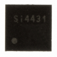
SI4431-A0-FM Silicon Laboratories Inc, SI4431-A0-FM Datasheet - Page 66

SI4431-A0-FM
Manufacturer Part Number
SI4431-A0-FM
Description
IC TXRX ISM 930MHZ 3.6V 20-QFN
Manufacturer
Silicon Laboratories Inc
Specifications of SI4431-A0-FM
Package / Case
20-QFN
Mfg Application Notes
Transitioning SI4430/31 to Rev B
Frequency
240MHz ~ 930MHz
Data Rate - Maximum
128kbps
Modulation Or Protocol
FSK, GFSK, OOK
Power - Output
13dBm
Sensitivity
-118dBm
Voltage - Supply
1.8 V ~ 3.6 V
Current - Receiving
18.5mA
Current - Transmitting
28mA
Data Interface
PCB, Surface Mount
Antenna Connector
PCB, Surface Mount
Operating Temperature
-40°C ~ 85°C
Number Of Receivers
2
Number Of Transmitters
1
Wireless Frequency
240 MHz to 930 MHz
Output Power
13 dBm
Operating Supply Voltage
1.8 V to 3.6 V
Maximum Operating Temperature
+ 85 C
Mounting Style
SMD/SMT
Maximum Supply Current
28 mA
Minimum Operating Temperature
- 40 C
Modulation
FSK, GFSK, OOK
Lead Free Status / RoHS Status
Lead free / RoHS Compliant
Applications
-
Memory Size
-
Lead Free Status / RoHS Status
Lead free / RoHS Compliant, Lead free / RoHS Compliant
Other names
336-1633-5
Available stocks
Company
Part Number
Manufacturer
Quantity
Price
Company:
Part Number:
SI4431-A0-FMR
Manufacturer:
SILICON
Quantity:
3 500
Part Number:
SI4431-A0-FMR
Manufacturer:
SILICONLABS/芯科
Quantity:
20 000
Si4431
8.8. GPIO Configuration
Three general purpose IOs (GPIOs) are available. Numerous functions such as specific interrupts, TRSW control,
Microcontroller Output, etc. can be routed to the GPIO pins as shown in the tables below. When in Shutdown mode
all the GPIO pads are pulled low.
Note: The ADC should not be selected as an input to the GPIO in Standby or Sleep Modes and will cause excess current con-
The GPIO settings for GPIO1 and GPIO2 are the same as for GPIO0 with the exception of the 00000 default
setting. The default settings for each GPIO are listed below:
The chip is configured to provide the System Clock output to the microcontroller so that only one crystal is needed
in the system, therefore reducing the BOM cost. For the TX Data Source, Direct Mode is used because long
packets are desired with a unique packet handling format already implemented in the microcontroller. In this
configuration the TX Data Clock is configured onto GPIO0, the TX Data is configured onto GPIO1, and the
Microcontroller System Clock output is configured onto GPIO2.
For a complete list of the available GPIO's see “Register 0Ch. GPIO Configuration 1,” on page 96, “Register 0Dh.
GPIO Configuration 2,” on page 97, and “Register 0Eh. I/O Port Configuration,” on page 98.
66
Add R/W Function/Des
0B
0C
0D
0E
sumption.
R/W
R/W
R/W
R/W
Configuration
Configuration
Configuration
Configuration
cription
I/O Port
GPIO0
GPIO1
GPIO2
gpio0drv[1] gpio0drv[0]
gpio1drv[1] gpio1drv[0]
gpio2drv[1] gpio2drv[0]
D7
GPIO0
GPIO1
GPIO2
GPIO
extitst[2]
D6
Preliminary Rev. 0.4
extitst[1] extitst[0]
pup0
pup1
pup2
D5
00000—Default Setting
Microcontroller Clock
gpio0[4] gpio0[3] gpio0[2] gpio0[1] gpio0[0]
gpio1[4] gpio1[3] gpio1[2] gpio1[1] gpio1[0]
gpio2[4] gpio2[3] gpio2[2] gpio2[1] gpio2[0]
POR Inverted
D4
POR
itsdo
D3
dio2
D2
dio1
D1
dio0
D0
POR Def.
00h
00h
00h
00h


