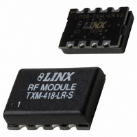
TXM-418-LR_ Linx Technologies Inc, TXM-418-LR_ Datasheet - Page 2

TXM-418-LR_
Manufacturer Part Number
TXM-418-LR_
Description
TRANSMITTER 418MHZ LR SERIES
Manufacturer
Linx Technologies Inc
Series
LRr
Datasheet
1.TXM-433-LR.pdf
(11 pages)
Specifications of TXM-418-LR_
Frequency
418MHz
Applications
ISM, RKE, Security and Fire Alarms
Modulation Or Protocol
ASK, OOK
Data Rate - Maximum
10 kbps
Power - Output
-4dBm ~ 4dBm
Current - Transmitting
3.3mA
Data Interface
PCB, Surface Mount
Antenna Connector
PCB, Surface Mount
Voltage - Supply
2.1 V ~ 3.6 V
Operating Temperature
-40°C ~ 85°C
Package / Case
Surface Mount
Board Size
12.7 mm x 9.1 mm x 3.3 mm
Minimum Operating Temperature
- 40 C
Supply Voltage (min)
2.1 V
Product
RF Modules
Maximum Frequency
418 MHz
Supply Voltage (max)
3.6 V
Maximum Operating Temperature
+ 85 C
Lead Free Status / RoHS Status
Lead free / RoHS Compliant
Features
-
Memory Size
-
Lead Free Status / Rohs Status
Lead free / RoHS Compliant
Other names
TXM-418-LR
Table 1: LR Series Transmitter Electrical Specifications
Notes
1. With a 50% duty cycle.
2. With a 750Ω resistor on LADJ.
3. See graph on Page 3.
4. Characterized, but not tested.
ABSOLUTE MAXIMUM RATINGS
Page 2
ELECTRICAL SPECIFICATIONS
Parameter
POWER SUPPLY
Operating Voltage
Supply Current:
Power-Down Current
TRANSMITTER•SECTION
Transmit Frequency Range:
Center Frequency Accuracy
Output Power
Output Power Control Range
Harmonic Emissions
Data Rate
Data Input:
Power Down Input:
ANTENNA PORT
RF Output Impedance
TIMING
Transmitter Turn-On Time:
ENVIRONMENTAL
Operating Temperature Range
Logic High
Logic Low
TXM-315-LR
TXM-418-LR
TXM-433-LR
Logic Low
Logic High
Logic Low
Logic High
Via V
Modulation Delay
CC
or PDN
Supply Voltage V
Any Input or Output Pin
Operating Temperature
Storage Temperature
Soldering Temperature
*NOTE*
damage to the device. Furthermore, extended operation at these maximum
ratings may reduce the life of this device.
Exceeding any of the limits of this section may lead to permanent
CC
Designation
R
V
I
V
V
I
PDN
F
P
P
V
V
CC
OUT
–
–
–
–
–
–
CC
IH
IH
C
O
H
IL
IL
V
V
CC
CC
Min.
2.1
-50
-80
DC
-40
-4
–
–
–
–
–
–
–
–
–
-0.25
–
-0.25
–
–
–
-0.3
-0.3
-40
-40
+225°C for 10 seconds
Typical
433.92
315
418
3.0
3.4
5.1
1.8
5.0
0.0
1.0
50
–
–
–
–
–
–
–
–
–
–
to
to V
to
to
10,000
Max.
0.25
0.25
30.0
CC
+50
+10
+85
3.6
-36
+4
–
–
–
–
–
–
–
–
–
–
–
+3.6
+85
+90
+ 0.3
mSec
Units
VDC
VDC
VDC
VDC
VDC
MHz
MHz
MHz
dBm
kHz
dBc
mA
mA
mA
bps
nA
dB
nS
°
Ω
VDC
VDC
C
°C
°C
Notes
1,2
–
2
–
–
–
–
–
–
2
3
–
–
–
–
–
–
4
4
4
4
PERFORMANCE DATA
TYPICAL PERFORMANCE GRAPHS
These performance parameters
are based on module operation at
25°C from a 3.0VDC supply unless
otherwise
illustrates
necessary
operation. It is recommended all
ground pins be connected to the
ground plane.
Figure 3: Modulation Delay
Figure 4: Output Power vs. LADJ Resistance
Figure 5: Current Consumption vs. Output Power (50% Duty Cycle)
4.5
3.5
2.5
3
4
2
6.00
12
10
noted.
8
6
4
2
0
9.00
for
the
1. 500mV/div
ASK RF Output
6.00
3.00
TX Data
testing
connections
3.00
Figure
0.00
2. 2.00V/div
0.00
-3.00
and
-3.00
Output Power (dBm)
100nS/div
Output Power (dBm)
2
-6.00
-6.00
Figure 2: Test / Basic Application Circuit
-9.00
VCC
-9.00
750
-12.00
-12.00
-15.00
-15.00
GND
DATA
GND
LADJ/VCC
-18.00
-18.00
-21.00
1
2
-21.00
GND
PDN
VCC
ANT
VCC
Page 3


