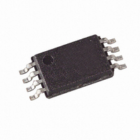
T48C862M-R4-TNS Atmel, T48C862M-R4-TNS Datasheet - Page 68

T48C862M-R4-TNS
Manufacturer Part Number
T48C862M-R4-TNS
Description
IC MON TIRE PRESS 433MHZ 24-SOIC
Manufacturer
Atmel
Datasheet
1.T48C862M-R4-TNS.pdf
(107 pages)
Specifications of T48C862M-R4-TNS
Frequency
433MHz
Modulation Or Protocol
FM, FSK
Data Rate - Maximum
32 kBaud
Power - Output
10dBm
Current - Transmitting
9.5mA
Data Interface
PCB, Surface Mount
Antenna Connector
PCB, Surface Mount
Memory Size
1KB EEPROM, 1KB RAM
Voltage - Supply
2 V ~ 4 V
Operating Temperature
-40°C ~ 125°C
Package / Case
24-SOIC (0.200", 5.30mm Width)
Lead Free Status / RoHS Status
Contains lead / RoHS non-compliant
Features
-
Applications
-
General SSI Operation
68
T48C862-R4 [Preliminary]
Figure 64. Block Diagram of the Synchronous Serial Interface
The SSI is comprised essentially of an 8-bit shift register with two associated 8-bit buff-
ers – the receive buffer (SRB) for capturing the incoming serial data and a transmit
buffer (STB) for intermediate storage of data to be serially output. Both buffers are
directly accessable by software. Transferring the parallel buffer data into and out of the
shift register is controlled automatically by the SSI control, so that both single byte trans-
fers or continuous bit streams can be supported.
The SSI can generate the shift clock (SC) either from one of several on-chip clock
sources or accept an external clock. The external shift clock is output on, or applied to
the Port BP40. Selection of an external clock source is performed by the Serial Clock
Direction control bit (SCD). In the combinational modes, the required clock is selected
by the corresponding timer mode.
The SSI can operate in three data transfer modes – synchronous 8-bit shift mode, a
9-bit Multi-Chip Link Mode (MCL) ,or 8-bit pseudo MCL protocol (without acknowledge-
bit).
External SSI clocking is not supported in these modes. The SSI should thus generate
and has full control over the shift clock so that it can always be regarded as an MCL bus
master device.
All directional control of the external data port used by the SSI is handled automatically
and is dependent on the transmission direction set by the Serial Data Direction (SDD)
control bit. This control bit defines whether the SSI is currently operating in Transmit
(TX) mode or Receive (RX) mode.
Serial data is organized in 8-bit telegrams which are shifted with the most significant bit
first. In the 9-bit MCL mode, an additional acknowledge bit is appended to the end of the
telegram for handshaking purposes (see “MCL Bus Protocol” on page 72).
At the beginning of every telegram, the SSI control loads the transmit buffer into the shift
register and proceeds immediately to shift data serially out. At the same time, incoming
data is shifted into the shift register input. This incoming data is automatically loaded
into the receive buffer when the complete telegram has been received. Thus, data can
be simultaneously received and transmitted if required.
T1OUT
SYSCL
POUT
TOG2
SIC1
/2
SC
Shift_CL
SO
Transmit
Buffer
I/O-bus
SIC2
MSB
STB
SSI-Control
8-bit Shift Register
I/O-bus
SISC
SRB
Control
LSB
Receive
Buffer
Timer 2 / Timer 3
SI
INT3
SO
Output
SI
4551C–4BMCU–01/04
SCI
SC
MCL_SC
MCL_SD
SD


