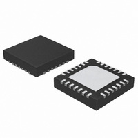
ATA5278-PKQI Atmel, ATA5278-PKQI Datasheet - Page 13

ATA5278-PKQI
Manufacturer Part Number
ATA5278-PKQI
Description
IC ANTENNA DVR STAND-ALONE 28QFN
Manufacturer
Atmel
Type
Stand Alone Antenna Driverr
Datasheet
1.ATA5278-PKQI.pdf
(34 pages)
Specifications of ATA5278-PKQI
Rf Type
TPM
Frequency
125kHz
Package / Case
28-VFQFN
Maximum Operating Temperature
+ 105 C
Mounting Style
SMD/SMT
Minimum Operating Temperature
- 40 C
Lead Free Status / RoHS Status
Lead free / RoHS Compliant
Features
-
Lead Free Status / Rohs Status
Lead free / RoHS Compliant
Other names
ATA5278-PKQITR
3.10
4832D–RKE–12/07
LF Data Modulation
Figure 3-8.
The buffer is structured into two parallel blocks with the same storage capacity. The reason for
this is that the LF data is handled as logical (e.g., Manchester coded) bits, where each data is
encoded by two so-called half bits. The minimum amount of data which can be written to or read
from the buffer is one logical bit, hence two half bits.
After activating the IC from power-down mode or any fault, the data pointer in
lowest point of the buffer (i.e., bit 190/191). Any write operation will store the data to the position
the pointer is pointing at, and moves it upwards one position. The data is always read from the
lowest point of the buffer by the modulator stage. Any read operation will cause the data in the
buffer to drop down one position, including the data pointer. Any further writes are ignored if the
data pointer reaches the upper border of the buffer, and the LF modulator stage stops operation
after the pointer has reached the lower border.
The LF modulator stage of the ATA5278 is fed with data from the LF data buffer. It is started
after a successfully received SPI command 11. Two half bits are loaded at a time and brought
sequentially to the driver control logic, starting with the half bit labeled lower in
applied for half the period time selected by the LF baud rate selector. Then the half bit labeled
upper is applied for the same time. The driver control stage generates a control signal for the
power output stages according to the input and the selected modulation mode. The IC has two
modulation modes, ASK and PSK. They are selected by the NASK_PSK bit (i.e., bit 0) in control
register 1. In ASK modulation mode (NASK_PSK = 0), the IC switches the carrier on and off
depending on the value of the half bit applied by the modulator stage, where 1 activates the car-
rier and 0 deactivates it. So if the carrier is to be activated for a certain time (i.e., continuous
wave), a corresponding amount of half bits have to be set to 1 in the LF data buffer.
on page 14
illustrates this behavior.
Structure Of Internal Data Buffer
AGND
LSB
6
5
4
3
2
1
MUX
4-1
Upper
Lower
Bit 188
Bit 190
Bit 0
Bit 2
.
.
.
.
.
.
.
.
.
Bit 189
Bit 191
Bit 1
Bit 3
.
.
.
.
.
.
.
.
.
Upper
Lower
Data pointer
modulator
stage
LF
Figure 3-8
ATA5278
Figure
Figure 3-9
3-8. It is
is at the
13


