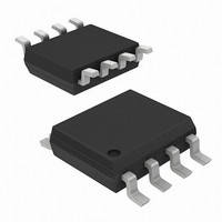
ATA556711-TASY Atmel, ATA556711-TASY Datasheet - Page 5

ATA556711-TASY
Manufacturer Part Number
ATA556711-TASY
Description
IC IDIC R/W 330BIT 0PF 8-SOIC
Manufacturer
Atmel
Series
ATA5567r
Datasheet
1.ATA556711N-DDT.pdf
(36 pages)
Specifications of ATA556711-TASY
Rf Type
Read / Write
Frequency
100kHz ~ 150kHz
Features
E5550, e5551, T5557 Binary Compatible
Package / Case
8-SOIC (0.154", 3.90mm Width)
Lead Free Status / RoHS Status
Lead free / RoHS Compliant
3.11
3.12
4874F–RFID–07/08
Memory
Traceability Data Structure
The memory is a 330-bit EEPROM, which is arranged in 10 blocks of 33 bits each. All 33 bits of
a block, including the lock bit, are programmed simultaneously.
Block 0 of page 0 contains the mode/configuration data, which is not transmitted during regu-
lar-read operations. Block 7 of page 0 may be used as a write protection password.
Bit 0 of every block is the lock bit for that block. Once locked, the block (including the lock bit
itself) is not re-programmable through the RF field.
Blocks 1 and 2 of page 1 contain traceability data and are transmitted with the modulation
parameters defined in the configuration register after the opcode “11” is issued by the reader
(see
Atmel.
Figure 3-3.
Blocks 1 and 2 of page 1 contain the traceability data and are programmed and locked by Atmel
during production testing
class (ACL) as defined in ISO/IEC 15963-1. The second byte is therefore defined as Atmel
manufacturer ID (15h). The following 8 bits are used as IC reference byte (ICR bits 47 to 40).
The 3 most significant bits define the IC version of the ATA5567, the foundry version, or both.
The lower 5 bits are by default reset (00) as the Atmel standard value. Other values may be
assigned, by request, to high volume customers as tag issuer identification.
The lower 40 bits of the data encode Atmel’s traceability information, and conform to a unique
numbering system. These 40 data bits are divided in two sub-groups, a 5-digit lot ID number,
and the binary wafer number (5 bits) concatenated with the sequential die number per wafer.
Note:
Figure 4-6 on page
1. This is only valid for sawn wafer “DDB, DDT” delivery.
Memory Map
(1)
11). These traceability data blocks are programmed and locked by
0
1
1
L
L
L
L
L
L
L
L
. The most significant byte of block 1 is fixed to E0h, the allocation
Not transmitted
1
User data or password
Configuration data
Traceability data
Traceability data
User data
User data
User data
User data
User data
User data
32 bits
32
Block 2
Block 1
Block 7
Block 6
Block 5
Block 4
Block 3
Block 2
Block 1
Block 0
ATA5567
®
’s
5


