TK5551M-PP Atmel, TK5551M-PP Datasheet - Page 7
TK5551M-PP
Manufacturer Part Number
TK5551M-PP
Description
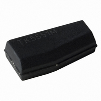
IC RFID 125KHZ READ/WRITE TAG
Manufacturer
Atmel
Series
TK5551r
Datasheet
1.TK5551M-PP.pdf
(12 pages)
Specifications of TK5551M-PP
Rf Type
Read / Write
Frequency
125kHz
Features
264-bit EEPROM
Package / Case
Plastic Package - 12mm L x 6mm W x 3mm H
Lead Free Status / RoHS Status
Contains lead / RoHS non-compliant


8. Writing Data into the TK5551
Figure 8-1.
9. Write Data Decoding
10. Actual Behavior of the Device
4709G–RFID–07/10
RF field
Read mode
Write Protocol
The write sequence of the TK5551 is shown below. Writing data into the transponder occurs by
interrupting the RF field with short gaps. After the start gap the standard write OP code (10) is
followed by the lock bit. The next 32 bits contain the actual data. The last 3 bits denote the des-
tination block address. If the correct number of bits have been received, the actual data is
programmed into the specified memory block.
The time elapsing between two detected gaps is used to encode the information. As soon as a
gap is detected, a counter starts counting the number of field clock cycles until the next gap is
detected. Depending on how many field clocks elapse, the data is regarded as “0” or “1”. The
required number of field clocks is shown in
counted clock periods is between 16 and 32, for a valid “1” it is 48 or 64 respectively. Any other
value being detected results in an error, and the device exits write mode and returns to read
mode.
Figure 9-1.
The TK5551 detects a gap if the voltage across the coils decreases below the threshold value of
an internal MOS transistor. Until then, the clock pulses are counted. The number given for a
valid “0” or “1” (see
there are always more clock pulses being counted than were applied by the base station. The
reason for this is the fact that an RF field cannot be switched off immediately. The coil voltage
decreases exponentially. So although the RF field coming from the base station is switched off,
it takes some time until the voltage across the coils reaches the threshold value of an internal
MOS transistor and the device detects the gap.
Referring to the following diagram (see
the times t
(e.g., field strength, etc.)
Field clock cycles
Write data decoder
Standard OP-code
Start gap
1
0 internal
0
Write Data Decoding Scheme
Write mode
and t
0
Figure
Lock bit
1
1 internal
fail
9-1) refers to the actual clock pulses counted by the device. However,
. The exact times for t
16
32 bit
0
Figure 10-1 on page
Figure
32
fail
9-1. A valid “0” is assumed if the number of
0
Address bits (e.g. block 4)
and t
1
48
1
8), this means that the device uses
are dependent on the application
0
1
0
64
writing done
> 64 clocks
TK5551
7
Related parts for TK5551M-PP
Image
Part Number
Description
Manufacturer
Datasheet
Request
R

Part Number:
Description:
Standard Read/write Id Transponder With Anti-collision
Manufacturer:
ATMEL Corporation
Datasheet:

Part Number:
Description:
DEV KIT FOR AVR/AVR32
Manufacturer:
Atmel
Datasheet:
Part Number:
Description:
INTERVAL AND WIPE/WASH WIPER CONTROL IC WITH DELAY
Manufacturer:
ATMEL Corporation
Datasheet:
Part Number:
Description:
Low-Voltage Voice-Switched IC for Hands-Free Operation
Manufacturer:
ATMEL Corporation
Datasheet:
Part Number:
Description:
MONOLITHIC INTEGRATED FEATUREPHONE CIRCUIT
Manufacturer:
ATMEL Corporation
Datasheet:
Part Number:
Description:
AM-FM Receiver IC U4255BM-M
Manufacturer:
ATMEL Corporation
Datasheet:
Part Number:
Description:
Monolithic Integrated Feature Phone Circuit
Manufacturer:
ATMEL Corporation
Datasheet:
Part Number:
Description:
Multistandard Video-IF and Quasi Parallel Sound Processing
Manufacturer:
ATMEL Corporation
Datasheet:
Part Number:
Description:
High-performance EE PLD
Manufacturer:
ATMEL Corporation
Datasheet:
Part Number:
Description:
8-bit Flash Microcontroller
Manufacturer:
ATMEL Corporation
Datasheet:
Part Number:
Description:
2-Wire Serial EEPROM
Manufacturer:
ATMEL Corporation
Datasheet: