CM200TU-5F Powerex Inc, CM200TU-5F Datasheet - Page 2
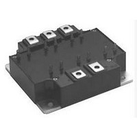
CM200TU-5F
Manufacturer Part Number
CM200TU-5F
Description
IGBT MOD 6PAC 250V 200A F SER
Manufacturer
Powerex Inc
Series
IGBTMOD™r
Type
IGBT Moduler
Datasheet
1.CM200TU-5F.pdf
(4 pages)
Specifications of CM200TU-5F
Igbt Type
Trench
Configuration
Three Phase Inverter
Voltage - Collector Emitter Breakdown (max)
250V
Vce(on) (max) @ Vge, Ic
1.7V @ 10V, 200A
Current - Collector (ic) (max)
200A
Current - Collector Cutoff (max)
1mA
Input Capacitance (cies) @ Vce
66nF @ 10V
Power - Max
600W
Input
Standard
Ntc Thermistor
No
Mounting Type
Chassis Mount
Package / Case
Module
Dc Collector Current
200A
Collector Emitter Voltage Vces
250V
Power Dissipation Pd
600W
Collector Emitter Voltage V(br)ceo
250V
Operating Temperature Range
-40°C To +150°C
No. Of Pins
17
Voltage
250V
Current
200A
Circuit Configuration
6-Pac
Rohs Compliant
Yes
Recommended Gate Driver
VLA504
Recommended Dc To Dc Converter
VLA106-15242 or VLA106-24242
Interface Circuit Ref Design
BG2B-3015 x3
Lead Free Status / RoHS Status
Lead free / RoHS Compliant


2
2
Powerex, Inc., 200 Hillis Street, Youngwood, Pennsylvania 15697-1800 (724) 925-7272
CM200TU-5F
Trench Gate Design Six IGBTMOD™
200 Amperes/250 Volts
Absolute Maximum Ratings, T
Ratings
Junction Temperature
Storage Temperature
Collector-Emitter Voltage (G-E SHORT)
Gate-Emitter Voltage (C-E SHORT)
Collector Current (T
Peak Collector Current (T
Emitter Current**
Peak Emitter Current**
Maximum Collector Dissipation (T
Mounting Torque, M5 Main Terminal
Mounting Torque, M5 Mounting
Weight
Isolation Voltage (Main Terminal to Baseplate, AC 1 min.)
Static Electrical Characteristics, T
Characteristics
Collector-Cutoff Current
Gate Leakage Voltage
Gate-Emitter Threshold Voltage
Collector-Emitter Saturation Voltage
Total Gate Charge
Emitter-Collector Voltage**
Dynamic Electrical Characteristics, T
Characteristics
Input Capacitance
Output Capacitance
Reverse Transfer Capacitance
Resistive
Load
Switch
Times
Diode Reverse Recovery Time**
Diode Reverse Recovery Charge**
Thermal and Mechanical Characteristics, T
Characteristics
Thermal Resistance, Junction to Case
Thermal Resistance, Junction to Case
Contact Thermal Resistance
* Pulse width and repetition rate should be such that the device junction temperature (T
**Represents characteristics of the anti-parallel, emitter-to-collector free-wheel diode (FWDi).
c
= 25 C)
Turn-on Delay Time
Rise Time
Turn-off Delay Time
Fall Time
j
150 C)
j
< 150 C)
j
= 25 C unless otherwise specified
j
R
V
R
= 25 C unless otherwise specified
V
Symbol
Symbol
Symbol
R
CE(sat)
t
th(j-c)
t
th(j-c)
I
I
C
GE(th)
C
V
C
d(on)
d(off)
CES
GES
th(c-f)
Q
Q
j
oes
t
EC
res
t
t
ies
rr
r
G
= 25 C unless otherwise specified
f
rr
Q
R
j
= 25 C unless otherwise specified
Per 1/6 Module, Thermal Grease Applied
V
I
Per Free-Wheel Diode 1/6 Module
I
C
CC
C
I
I
= 200A, V
= 200A, V
E
E
Load Switching Operation
= 100V, I
V
V
V
= 200A, di
= 200A, di
I
V
C
CC
Per IGBT 1/6 Module
I
CE
GE
V
R
E
CE
= 20mA, V
GE1
G
= 200A, V
Test Conditions
Test Conditions
= 100V, I
Test Conditions
= V
= V
= 13 , Resistive
= 10V, V
GE
= V
C
GE
CES
CES
j
= 200A, V
) does not exceed T
E
E
Symbol
= 10V, T
GE2
V
V
= 10V, T
/dt = -400A/ s
/dt = -400A/ s
T
V
I
I
, V
, V
CES
GES
CM
P
EM
I
I
T
stg
–
–
–
CE
C
iso
GE
C
E
GE
j
c
GE
CE
= 10V,
= 200A,
= 10V
= 0V
= 0V
= 0V
= 0V
j
j
GE
= 125 C
= 25 C
= 10V
j(max)
rating.
CM200TU-5F
Min.
Min.
Min.
-40 to 150
-40 to 125
–
–
3.0
–
–
–
–
–
–
–
–
–
–
–
–
–
–
–
–
2500
400*
400*
250
200
200
600
680
31
31
20
Typ.
Typ.
Typ.
–
–
4.0
1.2
1.1
–
–
–
–
–
–
–
–
–
–
–
0.09
1800
700
700
500
300
66
Max.
Max.
Max.
1
0.5
5.0
1.7
–
–
2.0
3.0
2.3
–
0.21
0.47
–
Amperes
Amperes
Amperes
Amperes
Grams
Watts
Units
Volts
Volts
Volts
Units
Units
Units
in-lb
in-lb
Volts
Volts
Volts
Volts
mA
C/W
C/W
C
C
nC
ns
ns
ns
ns
ns
nf
nf
nf
C/W
C
A
Related parts for CM200TU-5F
Image
Part Number
Description
Manufacturer
Datasheet
Request
R

Part Number:
Description:
IGBT MOD 6PAC 600V 200A F SER
Manufacturer:
Powerex Inc
Datasheet:

Part Number:
Description:
IGBT MOD 6PAC 600V 200A U SER
Manufacturer:
Powerex Inc
Datasheet:


Part Number:
Description:
THERMAL PAD
Manufacturer:
Laird Technologies
Datasheet:

Part Number:
Description:
Lamps 2.5V .35A Lens End
Manufacturer:
CHICAGO MINIATURE LIGHTING, LLC
Datasheet:
Part Number:
Description:
Lamps DISC BY CML 6/99
Manufacturer:
CHICAGO MINIATURE LIGHTING, LLC
Datasheet:
Part Number:
Description:
Lamps 2.5V .35A Lens End
Manufacturer:
CHICAGO MINIATURE LIGHTING, LLC
Datasheet:
Part Number:
Description:
Lamps DISC BY CML 2/99
Manufacturer:
CHICAGO MINIATURE LIGHTING, LLC
Datasheet:
Part Number:
Description:
Lamps LSNS ASSM 6.0/5.1V
Manufacturer:
CHICAGO MINIATURE LIGHTING, LLC
Datasheet:

Part Number:
Description:
Manufacturer:
Powerex Inc
Datasheet:
Part Number:
Description:
Manufacturer:
Powerex Inc
Datasheet:
Part Number:
Description:
Manufacturer:
Powerex Inc
Datasheet:
Part Number:
Description:
Manufacturer:
Powerex Inc
Datasheet:
Part Number:
Description:
Manufacturer:
Powerex Inc
Datasheet: