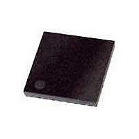
XR18W753IL48-F Exar Corporation, XR18W753IL48-F Datasheet - Page 8

XR18W753IL48-F
Manufacturer Part Number
XR18W753IL48-F
Description
IC RF TXRX 868-956MHZ 48QFN
Manufacturer
Exar Corporation
Type
RF Receiversr
Series
-r
Datasheet
1.XR18W753IL48-F.pdf
(27 pages)
Specifications of XR18W753IL48-F
Package / Case
48-VFQFN Exposed Pad
Frequency
868MHz ~ 954MHz
Data Rate - Maximum
250kbps
Modulation Or Protocol
DSSS
Applications
ISM
Power - Output
0dBm
Sensitivity
-94dBm
Voltage - Supply
2.2 V ~ 3.6 V
Current - Receiving
19mA
Current - Transmitting
22mA
Data Interface
PCB, Surface Mount
Antenna Connector
PCB, Surface Mount
Operating Temperature
-40°C ~ 85°C
Operating Frequency
100 KHz, 400 KHz
Operating Supply Voltage
2.2 V to 3.6 V
Maximum Operating Temperature
+ 85 C
Minimum Operating Temperature
- 40 C
Mounting Style
SMD/SMT
Noise Figure
12 dB
Supply Current
0.5 mA, 1.7 mA, 19 mA, 22 mA
Data Rate
250Kbps
Rf Ic Case Style
QFN
No. Of Pins
48
Supply Voltage Range
2.97V To 3.63V
Operating Temperature Range
-40°C To +85°C
Memory Size
-
Lead Free Status / RoHS Status
Lead free / RoHS Compliant
Lead Free Status / RoHS Status
Lead free / RoHS Compliant, Lead free / RoHS Compliant
Available stocks
Company
Part Number
Manufacturer
Quantity
Price
Part Number:
XR18W753IL48-F
Manufacturer:
EXAR/艾科嘉
Quantity:
20 000
XR18W753
SINGLE CHIP 868MHZ TO 956MHZ RF TRANSCEIVER
The XR18W753 is designed to operate in licensed-free European 868 MHz SRD, North American / Australian
915 MHz ISM, and 950 - 956 MHz bands.
The transmitter block is a direct-up-conversion I/Q modulator consisting of D/A converters, interpolation filters,
balanced I/Q mixers and a power amplifier.
The receiver is a Low-IF digital receiver consisting of a low-noise amplifier (LNA), I/Q mixers, IF filters, variable
gain amplifiers, and A/D converters.
The modem block is a Direct-Sequence-Spread-Spectrum (DSSS) O-QPSK digital modem with built-in
automatic gain control (AGC), Physical Layer Management Entity (PLME), Frame Check Sum (FCS)
computation, and Cyclical Redundancy Check (CRC) hardware.
The supporting block in the XR18W753 includes voltage/current reference, supply voltage stabilizer, and
crystal oscillator.
Interface to the XR18W753 can easily be made via the I
All internal registers and data buffers are accessible via this bus. A 16MHz CMOS clock is provided to the
microcontroller, eliminating the cost of an extra clock or crystal.
The I
bus interface consists of two lines: serial data (SDA) and serial clock (SCL). In the Standard-mode, the serial
clock and serial data can go up to 100 kbps and in the Fast-mode, the serial clock and serial data can go up to
400 kbps. The first byte sent by an I
when SCL is HIGH), 7-bit slave address and whether it is a read or write transaction. The next byte is the sub-
address that contains the address of the register to access. The XR18W751 responds to each write with an
acknowledge (SDA driven LOW by XR18W751 for one clock cycle when SCL is HIGH). If the TX FIFO is full,
the XR18W751 will respond with a negative acknowledge (SDA driven HIGH by XR18W751 for one clock
cycle when SCL is HIGH) when the CPU tries to write to the TX FIFO. The last byte sent by an I
is a stop bit (SDA transition from LOW to HIGH when SCL is HIGH). For complete details, see the I
specifications.
F
2.0 PRODUCT DESCRIPTION
2.1
2.2
2.3
2.4
2.5
2.6
2.6.1
IGURE
SDA
SCL
2
C-bus interface is compliant with the Standard-mode and Fast-mode I
5. I
Radio Frequency Standards
Transmitter Block
Receiver Block
Modem Block
Supporting Block
Baseband Microcontroller Interface
I
2
C-bus Interface
2
C S
START condition
TART AND
S
S
TOP
C
ONDITIONS
2
C-bus master contains a start bit (SDA transition from HIGH to LOW
8
2
C bus as in the XR18W750 baseband microcontroller.
2
C-bus specifications. The I
STOP condition
P
2
C-bus master
REV. 1.0.0
2
C-bus
2
C-


