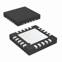
AD7298BCPZ Analog Devices Inc, AD7298BCPZ Datasheet - Page 18

AD7298BCPZ
Manufacturer Part Number
AD7298BCPZ
Description
IC ADC 12BIT SPI/SRL 1M 20LFCSP
Manufacturer
Analog Devices Inc
Datasheet
1.AD7298BCPZ.pdf
(24 pages)
Specifications of AD7298BCPZ
Data Interface
Serial, SPI™
Featured Product
AD7298 ADC with Temperature Sensor
Number Of Bits
12
Sampling Rate (per Second)
1M
Number Of Converters
1
Power Dissipation (max)
22.7mW
Voltage Supply Source
Single Supply
Operating Temperature
-40°C ~ 125°C
Mounting Type
Surface Mount
Package / Case
20-WFQFN, CSP Exposed Pad
Resolution (bits)
12bit
Sampling Rate
1MSPS
Input Channel Type
Single Ended
Supply Voltage Range - Digital
1.65V To 3.6V
Supply Current
5.8mA
Digital Ic Case
RoHS Compliant
Supply Voltage Range - Analog
1.65V To 3.6V
Digital Ic Case Style
LFCSP
Rohs Compliant
Yes
Lead Free Status / RoHS Status
Lead free / RoHS Compliant
Available stocks
Company
Part Number
Manufacturer
Quantity
Price
Company:
Part Number:
AD7298BCPZ
Manufacturer:
Analog Devices Inc
Quantity:
135
Part Number:
AD7298BCPZ
Manufacturer:
ADI/亚德诺
Quantity:
20 000
AD7298
REPEAT OPERATION
The REPEAT bit in the control register allows the user to select
a sequence of channels on which the AD7298 continuously
converts. When the REPEAT bit is set in the control register,
the AD7298 continuously cycles through the selected channels
in ascending order, beginning with the lowest channel and
converting all channels selected in the control register. On
completion of the sequence, the AD7298 returns to the first
selected channel in the control register and recommences the
sequence.
The conversion sequence of the selected channels in the repeat
mode of operation continues until such time as the control
register of the AD7298 is reprogrammed. If the T
selected in the control register, then the temperature conversion
will be available for conversion after the last analog input
channel in the sequence has been converted. It is not necessary
to write to the control register once a repeat operation is
initiated unless a change in the AD7298 configuration is
required. The WRITE bit must be set to zero or the DIN line
tied low to ensure that the control register is not accidentally
overwritten, or the automatic conversion sequence interrupted.
A write to the control register during the repeat mode of
operation resets the cycle even if the selected channels are
unchanged. Thus, the next conversion by the AD7298 after
a write operation will be the first selected channel in the
sequence.
DOUT
DOUT
SCLK
SCLK
DIN
DIN
CS
CS
1
1
REGISTER CH 0, CH 1, AND CH 2
DATA WRITTEN TO CONTROL
SELECTED: REPEAT = 1
CONVERSION RESULT
CONTROL REGISTER
NO WRITE TO THE
FOR CHANNEL 1
INVALID DATA
12
Figure 27. Configuring a Conversion and Read in Repeat Mode
16
16
SENSE
bit is
1
1
CONVERSION RESULT
CONTROL REGISTER
CONTROL REGISTER
Rev. A | Page 18 of 24
NO WRITE TO THE
NO WRITE TO THE
FOR CHANNEL 2
INVALID DATA
To select a sequence of channels, the associated channel bit
must be set to a logic high state (1) for each analog input whose
conversion is required. For example, if the REPEAT bit = 1,
then CH0, CH1, and CH2 = 1. The V
converted on the first CS falling edge following the write to
the control register, the V
subsequent CS falling edge, and the V
available for reading. The third CS falling edge following the
write operation initiates a conversion on V
result available for reading. The AD7298 operates with one
cycle latency, thus the conversion result corresponding to each
conversion is available one serial read cycle after the cycle in
which the conversion is initiated.
This mode of operation simplifies the operation of the device by
allowing consecutive channels to be converted without having
to reprogram the control register or write to the part on each
serial transfer. Figure 27 illustrates how to set up the AD7298
to continuously convert on a particular sequence of channels.
To exit the repeat mode of operation and revert back to the
traditional mode of operation of a multichannel ADC, ensure
that the REPEAT bit = 0 on the next serial write.
16
16
1
1
CONVERSION RESULT
CONVERSION RESULT
CONTROL REGISTER
CONTROL REGISTER
NO WRITE TO THE
NO WRITE TO THE
FOR CHANNEL 0
FOR CHANNEL 0
IN1
channel is converted on the
16
16
IN0
IN0
analog input is
conversion result is
IN2
and has the V
IN1


