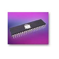
SST89V58RD2-33-C-TQJE Microchip Technology, SST89V58RD2-33-C-TQJE Datasheet - Page 33

SST89V58RD2-33-C-TQJE
Manufacturer Part Number
SST89V58RD2-33-C-TQJE
Description
IC MCU 8BIT 40KB FLASH 44TQFP
Manufacturer
Microchip Technology
Series
FlashFlex®r
Datasheet
1.SST89V54RD2-33-C-NJE.pdf
(77 pages)
Specifications of SST89V58RD2-33-C-TQJE
Program Memory Type
FLASH
Program Memory Size
32KB (32K x 8)
Package / Case
44-TQFP
Core Processor
8051
Core Size
8-Bit
Speed
33MHz
Connectivity
EBI/EMI, SPI, UART/USART
Peripherals
Brown-out Detect/Reset, POR, WDT
Number Of I /o
36
Eeprom Size
8K x 8
Ram Size
1K x 8
Voltage - Supply (vcc/vdd)
2.7 V ~ 3.6 V
Oscillator Type
External
Operating Temperature
0°C ~ 70°C
Processor Series
SST89xxxRD
Core
8051
Data Bus Width
8 bit
Data Ram Size
1 KB
Interface Type
SPI, UART
Maximum Clock Frequency
40 MHz
Number Of Programmable I/os
32
Number Of Timers
3
Maximum Operating Temperature
+ 70 C
Mounting Style
SMD/SMT
Minimum Operating Temperature
0 C
Lead Free Status / RoHS Status
Lead free / RoHS Compliant
Data Converters
-
Lead Free Status / Rohs Status
Lead free / RoHS Compliant
Available stocks
Company
Part Number
Manufacturer
Quantity
Price
Company:
Part Number:
SST89V58RD2-33-C-TQJE
Manufacturer:
Microchip Technology
Quantity:
10 000
FlashFlex MCU
SST89V54RD2/RD / SST89V58RD2/RD
4.0 FLASH MEMORY PROGRAMMING
The device internal flash memory can be programmed or
erased using the In-Application Programming (IAP) mode.
4.1 Product Identification
The Read-ID command accesses the Signature Bytes that
identify the device and the manufacturer as SST. External
programmers primarily use these Signature Bytes in the
selection of programming algorithms.
TABLE
4.2 In-Application Programming Mode
The device offers either 24/40 KByte of in-application pro-
grammable flash memory. During in-application program-
ming, the CPU of the microcontroller enters IAP mode. The
two blocks of flash memory allow the CPU to execute user
code from one block, while the other is being erased or
reprogrammed concurrently. The CPU may also fetch code
from an external memory while all internal flash is being
reprogrammed. The mailbox registers (SFST, SFCM,
SFAL, SFAH, SFDT and SFCF) located in the special func-
tion register (SFR), control and monitor the device’s erase
and program process.
Table 4-2 outline the commands and their associated mail-
box register settings.
4.2.1 In-Application Programming Mode Clock
Source
During IAP mode, both the CPU core and the flash control-
ler unit are driven off the external clock. However, an inter-
nal oscillator will provide timing references for Program and
Erase operations. The internal oscillator is only turned on
when required, and is turned off as soon as the flash oper-
ation is completed.
4.2.2 Memory Bank Selection for In-Application
Programming Mode
With the addressing range limited to 16 bit, only 64 KByte
of program address space is “visible” at any one time. The
bank selection (the configuration of EA# and SFCF[1:0]),
allows Block 1 memory to be overlaid on the lowest 8
KByte of Block 0 memory, making Block 1 reachable. The
©2007 Silicon Storage Technology, Inc.
Manufacturer’s ID
Device ID
SST89V54RD2/RD
SST89V58RD2/RD
4-1: Product Identification
Address
30H
31H
31H
T4-1.2 1255
Data
BFH
9EH
9AH
33
same concept is employed to allow both Block 0 and Block
1 flash to be accessible to IAP operations. Code from a
block that is not visible may not be used as a source to pro-
gram another address. However, a block that is not “visible”
may be programmed by code from the other block through
mailbox registers.
The device allows IAP code in one block of memory to pro-
gram the other block of memory, but may not program any
location in the same block. If an IAP operation originates
physically from Block 0, the target of this operation is implic-
itly defined to be in Block 1. If the IAP operation originates
physically from Block 1, then the target address is implicitly
defined to be in Block 0. If the IAP operation originates from
external program space, then, the target will depend on the
address and the state of bank selection.
4.2.3 IAP Enable Bit
The IAP enable bit, SFCF[6], enables in-application pro-
gramming mode. Until this bit is set, all flash programming
IAP commands will be ignored.
4.2.4 In-Application Programming Mode
Commands
All of the following commands can only be initiated in the
IAP mode. In all situations, writing the control byte to the
SFCM register will initiate all of the operations. All com-
mands will not be enabled if the security locks are enabled
on the selected memory block.
The Program command is for programming new data into
the memory array. The portion of the memory array to be
programmed should be in the erased state, FFH. If the
memory is not erased, it should first be erased with an
appropriate Erase command. Warning: Do not attempt to
write (program or erase) to a block that the code is cur-
rently fetching from. This will cause unpredictable pro-
gram behavior and may corrupt program data.
S71255-10-000
Data Sheet
12/07


