EFM32G200F16 Energy Micro, EFM32G200F16 Datasheet - Page 31
EFM32G200F16
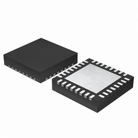
Manufacturer Part Number
EFM32G200F16
Description
MCU 32BIT 16KB FLASH 32-QFN
Manufacturer
Energy Micro
Series
Geckor
Datasheets
1.EFM32G200F16.pdf
(63 pages)
2.EFM32G200F16.pdf
(10 pages)
3.EFM32G200F16.pdf
(463 pages)
4.EFM32G200F16.pdf
(136 pages)
Specifications of EFM32G200F16
Core Processor
ARM® Cortex-M3™
Core Size
32-Bit
Speed
32MHz
Connectivity
EBI/EMI, I²C, IrDA, SmartCard, SPI, UART/USART
Peripherals
Brown-out Detect/Reset, DMA, POR, PWM, WDT
Number Of I /o
24
Program Memory Size
16KB (16K x 8)
Program Memory Type
FLASH
Ram Size
8K x 8
Voltage - Supply (vcc/vdd)
1.8 V ~ 3.8 V
Data Converters
A/D 4x12b, D/A 1x12b
Oscillator Type
External
Operating Temperature
-40°C ~ 85°C
Package / Case
32-VQFN Exposed Pad
Processor Series
EFM32G200
Core
ARM Cortex-M3
Data Bus Width
32 bit
Data Ram Size
8 KB
Interface Type
I2C, UART
Maximum Clock Frequency
32 MHz
Number Of Programmable I/os
24
Number Of Timers
2
Operating Supply Voltage
1.8 V to 3.8 V
Maximum Operating Temperature
+ 85 C
Mounting Style
SMD/SMT
Minimum Operating Temperature
- 40 C
Lead Free Status / RoHS Status
Lead free / RoHS Compliant
Eeprom Size
-
Lead Free Status / Rohs Status
Details


7.3.6 Erase and Write Operations
2010-09-06 - d0001_Rev1.00
false. The instructions in the block then appear to execute in zero cycles. With this scheme, performance
is optimized at the cost of higher energy consumption as the processor fetches more instructions from
memory than it actually executes. To disable the mode, write a 1 to the DISFOLD bit in the NVIC Auxiliary
Control Register; see the Cortex-M3 Technical Reference Manual for details. Normally, it is expected
that this feature is most efficient at core frequencies above 16 MHz. Folding is enabled by default.
Both page erase and write operations require that the address is written into the MSC_ADDRB register.
For erase operations, the address may be any within the page to be erased. Load the address by
writing 1 to the LADDRIM bit in the MSC_WRITECMD register. The LADDRIM bit only has to be written
once when loading the first address. After each word is written the internal address register ADDR
will be incremented automatically by 4. The INVADDR bit of the MSC_STATUS register is set if the
loaded address is outside the flash and the LOCKED bit of the MSC_STATUS register is set if the
page addressed is locked. Any attempts to command erase of or write to the page are ignored if
INVADDR or the LOCKED bits of the MSC_STATUS register are set. To abort an ongoing erase, set
the ERASEABORT bit in the MSC_WRITECMD register.
When a word is written to the MSC_WDATA register, the WDATAREADY bit of the MSC_STATUS
register is cleared. When this status bit is set, software or DMA may write the next word.
A single word write is commanded by setting the WRITEONCE bit of the MSC_WRITECMD register.
The operation is complete when the BUSY bit of the MSC_STATUS register is cleared and control of
the flash is handed back to the AHB interface, allowing application code to resume execution.
For a DMA write the software must write the first word to the MSC_WDATA register and then set the
WRITETRIG bit of the MSC_WRITECMD register. DMA triggers when the WDATAREADY bit of the
MSC_STATUS register is set.
It is possible to write words twice between each erase by keeping at 1 the bits that are not to be changed.
Let us take as an example writing two 16 bit values, 0xAAAA and 0x5555. To safely write them in the
same flash word this method can be used:
• Write 0xFFFFAAAA (word in flash becomes 0xFFFFAAAA)
• Write 0x5555FFFF (word in flash becomes 0x5555AAAA)
Note
The WRITEONCE, WRITETRIG and ERASEPAGE bits in the MSC_WRITECMD register
cannot safely be written from code in Flash. It is recommended to place a small code
section in RAM to set these bits and wait for the operation to complete. Also note that
DMA transfers to or from any other address in Flash while a write or erase operation is in
progress will produce unpredictable results.
...the world's most energy friendly microcontrollers
31
www.energymicro.com
Related parts for EFM32G200F16
Image
Part Number
Description
Manufacturer
Datasheet
Request
R

Part Number:
Description:
KIT STARTER EFM32 GECKO
Manufacturer:
Energy Micro
Datasheet:

Part Number:
Description:
KIT DEV EFM32 GECKO LCD SUPPORT
Manufacturer:
Energy Micro
Datasheet:

Part Number:
Description:
BOARD PROTOTYPING FOR EFM32
Manufacturer:
Energy Micro
Datasheet:

Part Number:
Description:
KIT DEVELOPMENT EFM32 GECKO
Manufacturer:
Energy Micro
Datasheet:

Part Number:
Description:
MCU, MPU & DSP Development Tools TG840 Sample Kit
Manufacturer:
Energy Micro
Datasheet:

Part Number:
Description:
MCU, MPU & DSP Development Tools TG Starter Kit
Manufacturer:
Energy Micro
Datasheet:
Part Number:
Description:
MCU, MPU & DSP Development Tools TG108 Sample Kit
Manufacturer:
Energy Micro
Part Number:
Description:
MCU, MPU & DSP Development Tools TG210 Sample Kit
Manufacturer:
Energy Micro
Datasheet:
Part Number:
Description:
MCU, MPU & DSP Development Tools TG822 Sample Kit
Manufacturer:
Energy Micro
Datasheet:
Part Number:
Description:
MCU, MPU & DSP Development Tools TG230 Sample Kit
Manufacturer:
Energy Micro

Part Number:
Description:
SAMPLE KIT (SMALL BOX - CONTAINING 2 DEVICES)
Manufacturer:
Energy Micro
Part Number:
Description:
SAMPLE KIT (SMALL BOX - CONTAINING 2 DEVICES)
Manufacturer:
Energy Micro