S9S08LG32J0VLK Freescale Semiconductor, S9S08LG32J0VLK Datasheet
S9S08LG32J0VLK
Specifications of S9S08LG32J0VLK
Available stocks


Related parts for S9S08LG32J0VLK

S9S08LG32J0VLK Summary of contents
Page 1
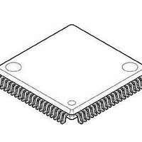
... Freescale reserves the right to change the detail specifications as may be required to permit improvements in the design of its products. © Freescale Semiconductor, Inc., 2009. All rights reserved. Document Number: MC9S08LG32 MC9S08LG32 80-LQFP Case 917A 14 mm × ...
Page 2
... Table 16.SPI Timing . . . . . . . . . . . . . . . . . . . . . . . . . . . . . . . . . . 31 Table 17.LCD Electricals Glass . . . . . . . . . . . . . . . . . . . . . 34 Table 18.Flash Characteristics . . . . . . . . . . . . . . . . . . . . . . . . . . 34 Table 19.Radiated Emissions, Electric Field . . . . . . . . . . . . . . . 35 Table 20.Conducted Susceptibility, EFT Table 21.Susceptibility Performance Classification . . . . . . . . . . 38 Table 22.Device Numbering System . . . . . . . . . . . . . . . . . . . . . 38 Table 23.Package Descriptions . . . . . . . . . . . . . . . . . . . . . . . . . 39 Table 24.Revision History MC9S08LG32 Series Data Sheet, Rev REFH DDAD ) . . . . . . . . . . . . . . . . . . . . . . . . . . . . . . . . . . . . . 27 Freescale Semiconductor = REFL ...
Page 3
... V SS VOLTAGE REGULATOR V SS2 V /V DDA REFH V /V SSA REFL Figure 1. MC9S08LG32 Series Block Diagram Freescale Semiconductor ON-CHIP ICE (ICE) and DEBUG MODULE (DBG) BKGD/MS Real Time Counter (RTC) TMRCLK Modulo Timer (MTIM) KBI[7:0] 8-BIT KEYBOARD INTERRUPT (KBI) SS RESET SPSCK SERIAL PERIPHERAL ...
Page 4
... This section shows the pin assignments for the MC9S08LG32 series devices. The priority of functions on a pin is in ascending order from left to right and bottom to top. Another view of pinouts and function priority is given in 4 MC9S08LG32 32,768 1984 yes yes yes yes 8 pin yes yes yes yes yes 2 6 yes MC9S08LG32 Series Data Sheet, Rev. 7 MC9S08LG16 18,432 Table 2 Freescale Semiconductor ...
Page 5
... PTB0/LCD29 14 PTD1/LCD1 15 PTD0/LCD0 CAP1 V 18 CAP2 V 19 LL1 V 20 LL2 V /V are internally connected to V REFH REFL Freescale Semiconductor 80-Pin LQFP Figure 2. 80-Pin LQFP NOTE /V . DDA SSA MC9S08LG32 Series Data Sheet, Rev. 7 Pin Assignments PTC4/LCD20 60 PTA0/LCD21 59 PTG2/LCD35 58 PTG3/LCD36 57 PTA1/SCL/LCD22 56 PTA2/SDA/ADC0/LCD23 55 PTA3/KBI4/TX2/ADC1/LCD24 ...
Page 6
... CAP2 V LL1 V LL2 V /V are internally connected to V REFH REFL 64-Pin LQFP Figure 3. 64-Pin LQFP NOTE /V . DDA SSA MC9S08LG32 Series Data Sheet, Rev. 7 PTC4/LCD20 48 PTA0/LCD21 47 PTG2/LCD35 46 PTG3/LCD36 45 PTA1/SCL/LCD22 44 PTA2/SDA/ADC0/LCD23 43 PTA3/KBI4/TX2/ADC1/LCD24 42 PTA4/KBI5/RX2/ADC2/LCD25 41 PTA5/KBI6/TPM2CH0/ADC3/LCD26 40 PTA6/KBI7/TPM2CH1/ADC4/LCD27 39 PTA7/TPMCLK/ADC5/LCD28 38 PTC5/BKGD/MS 37 PTC6/RESET 36 PTH4/RX1/KBI2/TPM1CH1/ADC10 35 PTH5/TX1/KBI3/TPM1CH0/ADC11 34 PTF3/SS/KBI0/TPM2CH5 33 Freescale Semiconductor ...
Page 7
... PTD6/LCD6 3 PTD5/LCD5 4 PTD4/LCD4 5 PTD3/LCD3 6 PTD2/LCD2 7 PTD1/LCD1 8 PTD0/LCD0 9 V CAP1 10 V CAP2 11 V LL1 V 12 LL2 are internally connected to V REFH REFL Freescale Semiconductor 48-Pin LQFP Figure 4. 48-Pin LQFP NOTE /V . DDA SSA MC9S08LG32 Series Data Sheet, Rev. 7 Pin Assignments 37 36 PTC4/LCD20 35 PTA0/LCD21 ...
Page 8
... TX2 — — — — — — — — — — — — — — — — KBI0 ADC15 IRQ Freescale Semiconductor Alt 4 — — — — — — — — — — — — — — — — — — ...
Page 9
... Freescale Semiconductor <-- Lowest Port Pin Alt 1 PTF1 RX1 TPM1CH0 PTF0 TX1 PTF3 SS PTH5 TX1 PTH4 RX1 PTH3 KBI7 PTH2 KBI6 PTH1 KBI5 PTH0 KBI4 PTC6 RESET PTC5 BKGD/MS PTA7 ...
Page 10
... Lowest Port Pin Alt 1 PTE3 LCD11 PTE2 LCD10 PTE1 LCD9 PTE0 LCD8 Table 3. Parameter Classifications NOTE MC9S08LG32 Series Data Sheet, Rev. 7 Priority --> Highest Alt 2 Alt 3 — — — — — — — — Freescale Semiconductor Alt 4 — — — — ...
Page 11
... Rating Operating temperature range (packaged) Maximum junction temperature Thermal resistance Single-layer board 80-pin LQFP 64-pin LQFP 48-pin LQFP Thermal resistance Four-layer board 80-pin LQFP 64-pin LQFP 48-pin LQFP The average chip-junction temperature (T Freescale Semiconductor Table 4. Absolute Maximum Ratings Rating Symbol stg ...
Page 12
... D J Table 6. ESD and Latch-Up Test Conditions Description Symbol R1 C — — — MC9S08LG32 Series Data Sheet, Rev. 7 and T ( neglected I (at equilibrium) D Equation 1 and Equation 2 Unit Value Ω 1500 100 pF 3 — –2.5 V 7.5 V Freescale Semiconductor Eqn. 2 Eqn. 3 iteratively ...
Page 13
... P Input low voltage; all digital inputs 9 P Input hysteresis; all digital inputs 10 P Input leakage current; input only pins 11 P High impedence (off-state) leakage current Internal pullup resistors 13 P Internal pulldown resistors Freescale Semiconductor 1 Rating Symbol V HBM V CDM = 85 ° LAT Table 8. DC Characteristics ...
Page 14
... load will shunt current greater than maximum DD Freescale Semiconductor Unit μ and could ...
Page 15
... Typical vs 0.8 Hot (105°C) Room (25°C) 0.6 Cold (-40°C) 0.4 0.2 0 -10 -11 -12 -13 -14 -15 I (mA) OH Figure 7. Typical High-side Drive (source) characteristics – High Drive (PTxDSn = 1) Freescale Semiconductor = 5V DD 1.40 1.20 1.00 0.80 0.60 0.40 0.20 0. 0.90 0.80 0.70 0.60 ...
Page 16
... Room (25°C) 1.0 Cold (-40°C) 0.8 0.6 0.4 0.2 0 (mA) OH Figure 8. Typical High-side Drive (source) characteristics – Low Drive (PTxDSn = 1.2 1.0 0.8 0.6 0.4 0.2 0 MC9S08LG32 Series Data Sheet, Rev. 7 Typical vs = Hot (105°C) Room (25°C) Cold (-40° (mA) OH Freescale Semiconductor ...
Page 17
... Wait mode supply current FEI mode, all modules off Stop2 mode supply current Stop3 mode supply current No clocks active Freescale Semiconductor Table 9. Supply Current Characteristics V Bus DD Symbol Freq ( MHz MHz 20 MHz 5 1 MHz RI 20 MHz MHz 20 MHz 5 1 MHz WI 20 MHz ...
Page 18
... Freescale Semiconductor Temp (°C) ...
Page 19
... Typical values are measured at 25 °C. Characterized, not tested. 2 LCD configured for Charge Pump Enabled V 3 This does not include current required for 32 kHz oscillator. 4 This is the maximum current when all LCD inputs/outputs are used Freescale Semiconductor Bus Symbol Freq — n/a LVD LVD connected to V ...
Page 20
... Electrical Characteristics I DD Figure 10. Typical Run Figure 11. Typical Run for FBE Mode at 20 MHz for FEE Mode at 1 MHz DD MC9S08LG32 Series Data Sheet, Rev. 7 Freescale Semiconductor ...
Page 21
... I DD Figure 12. Typical Run Freescale Semiconductor V DD for FEE Mode at 20 MHz Figure 13. Typical Stop2 I DD MC9S08LG32 Series Data Sheet, Rev. 7 Electrical Characteristics 21 ...
Page 22
... High range (RANGE = 1, HGO = 0) BLPE mode 2 D Load capacitors Figure 14. Typical Stop3 I Characteristic 2 MC9S08LG32 Series Data Sheet, Rev Symbol Min Typ Max f 32 — 38 — — 16 hi-hgo f 1 — 8 hi-lp C See crystal or resonator 1 C manufacturer’s recommendation. 2 Freescale Semiconductor Unit kHz MHz MHz MHz ...
Page 23
... This parameter is characterized and not tested on each device. 4 Proper PC board layout procedures must be followed to achieve specifications MHz crystal Figure 15. Typical Crystal or Resonator Circuit: High Range and Low Range/High Gain Freescale Semiconductor Characteristic ≥8 MHz 4 MHz 1 MHz 5 5 XOSC EXTAL ...
Page 24
... Jitter Jitter Freescale Semiconductor Unit kHz kHz μs MHz MHz %f dco %f dco %f dco %f dco mS %f dco . Bus percentage ...
Page 25
... DDAD Ground voltage Delta – SSAD Ref Voltage — High Ref Voltage — Low Input Voltage — Input — Capacitance Freescale Semiconductor ICS Trim values -40°C 25°C 110°C 1 Symb Min Typ V 2.7 — DDAD ΔV –100 0 DDAD ΔV –100 0 SSAD V — ...
Page 26
... V ADIN – INPUT PIN INPUT PIN INPUT PIN MC9S08LG32 Series Data Sheet, Rev. 7 Max Unit Comment 7 kΩ — kΩ External to MCU 8.0 MHz — 4.0 SIMPLIFIED CHANNEL SELECT CIRCUIT ADC SAR ENGINE R ADIN R ADIN R ADIN R ADIN C ADIN Freescale Semiconductor ...
Page 27
... Non-Linearity P 10-bit mode T 8-bit mode 11 T Integral 12-bit mode Non-Linearity P 10-bit mode T 8-bit mode 12 T Zero-Scale 12-bit mode Error P 10-bit mode T 8-bit mode Freescale Semiconductor = V REFH Conditions Symb Min — I DDAD — I DDAD — I DDAD — I DDAD I DDAD f ADACK 1.25 t ...
Page 28
... LSB ±0.5 — — ±0.5 — — ±1 2 — — LSB ±0.2 ±2.5 — ±0.1 ±1 — — 1.646 — mV/°C — 1.769 — — 701.2 — mV Freescale Semiconductor Comment ADIN DDAD — 4 Pad leakage * R AS — — ...
Page 29
... This is the minimum pulse width that is guaranteed to pass through the pin synchronization circuitry. Shorter pulses may or may not be recognized. In stop mode, the synchronizer is bypassed so shorter pulses can be recognized. 5 Timing is shown with respect to 20 Except for LCD pins in Open Drain mode. RESET PIN Freescale Semiconductor Table 14. Control Timing Rating Symbol ) f Bus ...
Page 30
... TCLK t TCLK t clkh t clkl t ICPW t TCLK t clkh Figure 21. Timer External Clock t ICPW t ICPW Figure 22. Timer Input Capture Pulse MC9S08LG32 Series Data Sheet, Rev. 7 Min Max Unit Bus 4 — t cyc 1.5 — t cyc 1.5 — t cyc 1.5 — t cyc t clkl Freescale Semiconductor ...
Page 31
... D Data valid (after SPSCK edge) 9 Master Slave D Data hold time (outputs) 10 Master Slave D Rise time 11 Input Output D Fall time 12 Input Output Freescale Semiconductor describe the timing requirements for the SPI system. Table 16. SPI Timing Symbol SPSCK t Lead t Lag t WSPSCK dis ...
Page 32
... SS output mode (DDS7 = 1, SSOE = 1). 2. LSBF = 0. For LSBF = 1, bit order is LSB, bit 1, ..., bit 6, MSB BIT BIT Figure 23. SPI Master Timing (CPHA = BIT BIT Figure 24. SPI Master Timing (CPHA =1) MC9S08LG32 Series Data Sheet, Rev LSB IN 10 LSB OUT LSB IN MASTER LSB OUT PORT DATA Freescale Semiconductor ...
Page 33
... SPSCK (CPOL = 0) (INPUT) 4 SPSCK (CPOL = 1) (INPUT) 9 MISO SEE SLAVE NOTE 1 (OUTPUT MOSI MSB IN (INPUT) NOTE: 1. Not defined but normally LSB of character just received Freescale Semiconductor BIT BIT Figure 25. SPI Slave Timing (CPHA = BIT MSB OUT 6 BIT Figure 26. SPI Slave Timing (CPHA = 1) MC9S08LG32 Series Data Sheet, Rev ...
Page 34
... For more detailed DD Typical Max 5.5 5.5 200 5 6. 4000 20,000 4 — 6 — — — 100,000 — 100 — Freescale Semiconductor Units Unit V V kHz μs t Fcyc t Fcyc t Fcyc t Fcyc mA mA cycles years ...
Page 35
... Parameter Conducted susceptibility, electrical fast transient/burst (EFT/B) 1 Data based on qualification test results. Not tested in production. 2 Exceptions as covered in footnotes 3 and 4. Freescale Semiconductor Table 19. Radiated Emissions, Electric Field Conditions Frequency V = 5.5 0.15 – 50 MHz DD ...
Page 36
... Individual performance of each pin is shown in Figure 27. 4 MHz, Positive Polarity Pins 1 – 41 Note: RESET retested with 0.1 μF capacitor from pin to ground is Class A compliant as shown by 48*. Figure 28. 4 MHz, Positive Polarity Pins 42 – Figure 27, Figure 28, Figure 29, and MC9S08LG32 Series Data Sheet, Rev. 7 Figure 30. Freescale Semiconductor ...
Page 37
... Figure 29. 4 MHz, Negative Polarity Pins 1 – 41 Note: RESET retested with 0.1 μF capacitor from pin to ground is Class A compliant as shown by 48*. Figure 30. 4 MHz, Negative Polarity Pins 42 – 80 Freescale Semiconductor MC9S08LG32 Series Data Sheet, Rev. 7 Electrical Characteristics 37 ...
Page 38
... D Hard failure E Damage 3 Ordering Information This section contains ordering information for MC9S08LG32 and MC9S08LG16 devices. Memory 1 Device Number FLASH S9S08LG32J0CLK 32 KB S9S08LG32J0CLH S9S08LG32J0CLF S9S08LG32J0VLK 32 KB S9S08LG32J0VLH S9S08LG32J0VLF S9S08LG16J0VLH 18 KB S9S08LG16J0VLF MC9S08LG32CLK 32 KB MC9S08LG32CLH MC9S08LG32CLF MC9S08LG16CLH 18 KB MC9S08LG16CLF 1 See the MC9S08LG32 Reference Manual (document MC9S08LG32RM), for a complete description of modules included on each device ...
Page 39
... Low Quad Flat Package 4.1 Mechanical Drawings The following pages are mechanical drawings for the packages described in available drawings please visit our web site (http://www.freescale.com) and enter the package’s document number into the keyword search box. Freescale Semiconductor S08 X ...
Page 40
... Package Information 4.1.1 80-pin LQFP 40 MC9S08LG32 Series Data Sheet, Rev. 7 Freescale Semiconductor ...
Page 41
... Freescale Semiconductor MC9S08LG32 Series Data Sheet, Rev. 7 Package Information 41 ...
Page 42
... Package Information Figure 33. 80-pin LQFP Package Drawing (Case 917A, Doc #98ASS23237W) 42 MC9S08LG32 Series Data Sheet, Rev. 7 Freescale Semiconductor ...
Page 43
... LQFP Freescale Semiconductor MC9S08LG32 Series Data Sheet, Rev. 7 Package Information 43 ...
Page 44
... Package Information 44 MC9S08LG32 Series Data Sheet, Rev. 7 Freescale Semiconductor ...
Page 45
... Figure 34. 64-pin LQFP Package Drawing (Case 840F, Doc #98ASS23234W) Freescale Semiconductor MC9S08LG32 Series Data Sheet, Rev. 7 Package Information 45 ...
Page 46
... Package Information 4.1.3 48-pin LQFP 46 MC9S08LG32 Series Data Sheet, Rev. 7 Freescale Semiconductor ...
Page 47
... Figure 35. 48-pin LQFP Package Drawing (Case 932, Doc #98ASH00962A) Freescale Semiconductor MC9S08LG32 Series Data Sheet, Rev. 7 Package Information 47 ...
Page 48
... Updated auto part numbers, changed TCLK, T0CH0, T0CH1, T1CH0, T1CH1, T1CH2, T1CH3, T1CH3, T1CH4, and T1CH5 to TPMCLK, TPM0CH0, TPM0CH1,TPM1CH0, TPM1CH1, TPM1CH2, TPM1CH3, TPM1CH4, and TPM1CH5, and changed the maximum LCD frame frequency to 64 Hz. 48 Table 24. Revision History Description of Changes MC9S08LG32 Series Data Sheet, Rev. 7 Table 19 and Table 20. Freescale Semiconductor ...
Page 49
... Freescale Semiconductor THIS PAGE INTENTIONALLY BLANK MC9S08LG32 Series Data Sheet, Rev ...
Page 50
... Freescale Semiconductor product could create a situation where personal injury or death may occur. Should Buyer ...