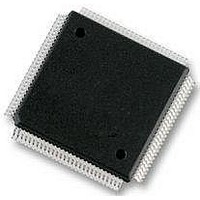
S912XEQ384J3CAL Freescale Semiconductor, S912XEQ384J3CAL Datasheet - Page 539

S912XEQ384J3CAL
Manufacturer Part Number
S912XEQ384J3CAL
Description
IC MCU 16BIT 384KB FLASH 112LQFP
Manufacturer
Freescale Semiconductor
Series
HCS12r
Datasheet
1.S912XEQ384J3CAL.pdf
(1328 pages)
Specifications of S912XEQ384J3CAL
Core Processor
HCS12X
Core Size
16-Bit
Speed
50MHz
Connectivity
CAN, EBI/EMI, I²C, IrDA, SCI, SPI
Peripherals
LVD, POR, PWM, WDT
Number Of I /o
91
Program Memory Size
384KB (384K x 8)
Program Memory Type
FLASH
Eeprom Size
4K x 8
Ram Size
24K x 8
Voltage - Supply (vcc/vdd)
1.72 V ~ 5.5 V
Data Converters
A/D 16x12b
Oscillator Type
External
Operating Temperature
-40°C ~ 85°C
Package / Case
112-LQFP
Core
HCS12X
Data Bus Width
16 bit
Data Ram Size
24 KB
Interface Type
SCI, SPI, I2C, CAN
Maximum Clock Frequency
50 MHz
Number Of Programmable I/os
91
Number Of Timers
1
Operating Supply Voltage
3.13 V to 5.5 V
Maximum Operating Temperature
+ 260 C
Mounting Style
SMD/SMT
Lead Free Status / RoHS Status
Lead free / RoHS Compliant
Available stocks
Company
Part Number
Manufacturer
Quantity
Price
Company:
Part Number:
S912XEQ384J3CAL
Manufacturer:
Freescale Semiconductor
Quantity:
10 000
- Current page: 539 of 1328
- Download datasheet (9Mb)
14.3.2.4
Read or write: Anytime
All bits reset to zero.
14.3.2.5
Freescale Semiconductor
Module Base + 0x0003
Module Base + 0x0004
OC7M[7:0]
OC7D[7:0]
Because of an order from the United States International Trade Commission, BGA-packaged product lines and partnumbers
Reset
Reset
indicated here currently are not available from Freescale for import or sale in the United States prior to September 2010
Field
Field
7:0
7:0
W
W
R
R
TCNT15
OC7D7
Output Compare Mask Action for Channel 7:0
A channel 7 event, which can be a counter overflow when TTOV[7] is set or a successful output compare
on channel 7, overrides any channel 6:0 compares. For each OC7M bit that is set,the output compare
action reflects the corresponding OC7D bit.
0 The corresponding OC7Dx bit in the output compare 7 data register will not be transferred to the timer port on
1 The corresponding OC7Dx bit in the output compare 7 data register will be transferred to the timer port on a
Note: The corresponding channel must also be setup for output compare (IOSx = 1 andOCPDx = 0) for data to
Output Compare 7 Data Bits — A channel 7 event, which can be a counter overflow when TTOV[7] is set or A
channel 7 output compare can cause bits in the output compare 7 data register to transfer to the timer port data
register depending on the output compare 7 mask register.
Output Compare 7 Data Register (OC7D)
Timer Count Register (TCNT)
15
0
0
7
a channel 7 event, even if the corresponding pin is setup for output compare.
channel 7 event.
be transferred from the output compare 7 data register to the timer port.
TCNT14
OC7D6
14
0
0
6
Figure 14-6. Output Compare 7 Data Register (OC7D)
Figure 14-7. Timer Count Register High (TCNT)
MC9S12XE-Family Reference Manual Rev. 1.23
Table 14-4. OC7M Field Descriptions
Table 14-5. OC7D Field Descriptions
TCNT13
OC7D5
13
5
0
0
TCNT12
OC7D4
12
0
0
4
Description
Description
TCNT11
OC7D3
11
0
0
3
Chapter 14 Enhanced Capture Timer (ECT16B8CV3)
TCNT10
OC7D2
10
2
0
0
OC7D1
TCNT9
0
0
1
9
OC7D0
TCNT8
0
0
0
8
539
Related parts for S912XEQ384J3CAL
Image
Part Number
Description
Manufacturer
Datasheet
Request
R
Part Number:
Description:
Manufacturer:
Freescale Semiconductor, Inc
Datasheet:
Part Number:
Description:
Manufacturer:
Freescale Semiconductor, Inc
Datasheet:
Part Number:
Description:
Manufacturer:
Freescale Semiconductor, Inc
Datasheet:
Part Number:
Description:
Manufacturer:
Freescale Semiconductor, Inc
Datasheet:
Part Number:
Description:
Manufacturer:
Freescale Semiconductor, Inc
Datasheet:
Part Number:
Description:
Manufacturer:
Freescale Semiconductor, Inc
Datasheet:
Part Number:
Description:
Manufacturer:
Freescale Semiconductor, Inc
Datasheet:
Part Number:
Description:
Manufacturer:
Freescale Semiconductor, Inc
Datasheet:
Part Number:
Description:
Manufacturer:
Freescale Semiconductor, Inc
Datasheet:
Part Number:
Description:
Manufacturer:
Freescale Semiconductor, Inc
Datasheet:
Part Number:
Description:
Manufacturer:
Freescale Semiconductor, Inc
Datasheet:
Part Number:
Description:
Manufacturer:
Freescale Semiconductor, Inc
Datasheet:
Part Number:
Description:
Manufacturer:
Freescale Semiconductor, Inc
Datasheet:
Part Number:
Description:
Manufacturer:
Freescale Semiconductor, Inc
Datasheet:
Part Number:
Description:
Manufacturer:
Freescale Semiconductor, Inc
Datasheet:


