A5191HRTLG-XTD ON Semiconductor, A5191HRTLG-XTD Datasheet - Page 8
A5191HRTLG-XTD
Manufacturer Part Number
A5191HRTLG-XTD
Description
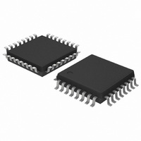
MODEM HART SGL CMOS 32-LQFP
Manufacturer
ON Semiconductor
Datasheet
1.A5191HRTPG-XTD.pdf
(14 pages)
Specifications of A5191HRTLG-XTD
Data Format
HART
Interface
CMOS
Voltage - Supply
3 V ~ 5.5 V
Mounting Type
Surface Mount
Package / Case
32-LQFP
Logic Type
CMOS Modem
Logic Family
A5191HRT
Input Level
CMOS
Supply Voltage (max)
5 V
Supply Voltage (min)
3.3 V
Maximum Operating Temperature
+ 85 C
Function
Use in highway addressable remote transducer (HART) field instruments and masters
Minimum Operating Temperature
- 40 C
Mounting Style
SMD/SMT
Supply Voltage Range
3V To 5.5V
Operating Temperature Range
-40°C To +85°C
Digital Ic Case Style
LQFP
No. Of Pins
32
Msl
MSL 3 - 168 Hours
Filter Terminals
SMD
No. Of I/o's
1
Rohs Compliant
Yes
Communication Function
HART Modem
Lead Free Status / RoHS Status
Lead free / RoHS Compliant
Baud Rates
-
Lead Free Status / Rohs Status
Lead free / RoHS Compliant
Other names
766-1011
Available stocks
Company
Part Number
Manufacturer
Quantity
Price
Company:

Part Number:
A5191HRTLG-XTD
Manufacturer:
ON
Quantity:
4 500
Company:
Part Number:
A5191HRTLG-XTD
Manufacturer:
ON
Quantity:
598
Company:
Part Number:
A5191HRTLG-XTD
Manufacturer:
ON Semiconductor
Quantity:
10 000
Part Number:
A5191HRTLG-XTD
Manufacturer:
ON/安森美
Quantity:
20 000


Functional Description
Highway Addressable Remote Transducer (HART) field
instruments and masters. The modem IC contains a transmit
data modulator with signal shaper, carrier detect circuitry, an
analog receiver, demodulator circuitry and a X-tall
oscillator, as shown in the block diagram in Figure 1.
and generates a sine shaped FSK modulated signal at the
analog output TxA. A digital “1” or mark is represented with
a frequency of 1200 Hz. A digital “0” or space is represented
with a frequency of 2200 Hz. The used bit rate is 1200 baud.
input, filters it with a band-pass filter and generates 2 digital
signals: RxD: Received Data and CD: Carrier Detect. At the
digital output RxD the original modulated signal is received.
CD outputs the Carrier Detect signal. It goes logic high if the
received signal is above 100 mVpp during 4 consecutive
carrier periods.
using either a simple external resonator or an external clock
source.
Detailed Description
Modulator
TxD input and generates the FSK modulated signal at the
TxA output.
1200 Hz. A logic “0”or space is represented by a frequency
fs = 2400 Hz.
RTS
TxD
The A5191HRT is a single-chip modem for use in
The modulator accepts digital data at its digital input TxD
The demodulator receives the FSK signal at its analog
The oscillator provides the modem with a stable time base
The modulator accepts digital data in NRZ form at the
A logic “1” or mark is represented by a frequency fm =
t
“1” = Mark
BIT
1.2 kHz
= 833 ms
Figure 5. Modulator Block Diagram
Controlled
Oscillator
Numeric
Figure 6. Modulation Timing
Shaper
Sine
“0” = Space
t
BIT
2.4 kHz
= 417 m s
MODULATOR
TxA
PC20101117.1
PC 20101013 .3
t
FSK_OUT
http://onsemi.com
8
continuous mode preventing abrupt phase shifts when
switching between mark and space frequency. The control
signal Request To Send RTSB enables the NCO. When
RTSB is logic low the modulator is active and A5191HRT
is in transmit mode. When RTSB is logic high the modulator
is disabled and A5191HRT is in receive mode.
Shaper block to a trapezoidal signal. This circuit controls the
rising and falling edge to be inside the standard HART
waveshape limits. Figure 7 shows the transmit-signal forms
captured at TxA for mark and space frequency. The slew
rates are SR
3300 V/s at the space frequency. For AREF = 1.235 V, TxA
will have a voltage swing from approximately 0.25 to 0.75
V
0.5 V
0.5 V
Demodulator
and reconstructs the original modulated signal at the RxD
output. Figure 8 illustrates the demodulation process.
frame with Start, Stop, 8 Data – and 1 Parity bit. The
communication speed is 1200 baud.
FSK_IN
RxD
V
PC20101013.4
V
DC
The Numeric Controlled Oscillator NCO works in a phase
The digital outputs of the NCO are shaped in the Sine
The demodulator accepts a FSK signal at the RxA input
This HART bit stream follows a standard 11-bit UART
Figure 7. Modulator shaped output signal for Mark
TxA
TxA
IDLE (mark)
.
0
0
Start
t
BIT
“0”
and Space frequency at TxA pin.
m
= 1860 V/s at the mark frequency and SR
Figure 8. Modulation Timing
LSB
D0
“1”
SR
“1” = Mark; f
“0” = Space; f
D1
“0”
s
= 3300 V/s
D2
“1”
1
8 data bits
1
SR
D3
“0”
m
m
s
=1.2 kHz
= 1860 V/s
=2.4 kHz
D4
“0”
D5
“1”
D6
“0”
MSB
D7
“1”
2
2
Par
“0”
0.5 V
Stop
PC20101118.1
t
BIT
0.5 V
IDLE (mark)
t (ms)
t (ms)
s
=
Related parts for A5191HRTLG-XTD
Image
Part Number
Description
Manufacturer
Datasheet
Request
R

Part Number:
Description:
ON Semiconductor [VOLTAGE REGULATOR]
Manufacturer:
ON Semiconductor
Datasheet:
Part Number:
Description:
357-036-542-201 CARDEDGE 36POS DL .156 BLK LOPRO
Manufacturer:
ON Semiconductor
Datasheet:
Part Number:
Description:
357-036-542-201 CARDEDGE 36POS DL .156 BLK LOPRO
Manufacturer:
ON Semiconductor
Datasheet:
Part Number:
Description:
357-036-542-201 CARDEDGE 36POS DL .156 BLK LOPRO
Manufacturer:
ON Semiconductor
Datasheet:
Part Number:
Description:
357-036-542-201 CARDEDGE 36POS DL .156 BLK LOPRO
Manufacturer:
ON Semiconductor
Datasheet:
Part Number:
Description:
357-036-542-201 CARDEDGE 36POS DL .156 BLK LOPRO
Manufacturer:
ON Semiconductor
Datasheet:
Part Number:
Description:
357-036-542-201 CARDEDGE 36POS DL .156 BLK LOPRO
Manufacturer:
ON Semiconductor
Datasheet:
Part Number:
Description:
357-036-542-201 CARDEDGE 36POS DL .156 BLK LOPRO
Manufacturer:
ON Semiconductor
Datasheet:
Part Number:
Description:
357-036-542-201 CARDEDGE 36POS DL .156 BLK LOPRO
Manufacturer:
ON Semiconductor
Datasheet:
Part Number:
Description:
357-036-542-201 CARDEDGE 36POS DL .156 BLK LOPRO
Manufacturer:
ON Semiconductor
Datasheet:
Part Number:
Description:
357-036-542-201 CARDEDGE 36POS DL .156 BLK LOPRO
Manufacturer:
ON Semiconductor
Datasheet:
Part Number:
Description:
Manufacturer:
ON Semiconductor
Datasheet:
Part Number:
Description:
Manufacturer:
ON Semiconductor
Datasheet:
Part Number:
Description:
Manufacturer:
ON Semiconductor
Datasheet: