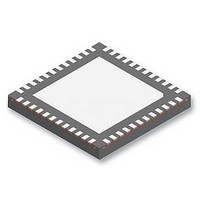
DS92LV2421SQE/NOPB National Semiconductor, DS92LV2421SQE/NOPB Datasheet - Page 7

DS92LV2421SQE/NOPB
Manufacturer Part Number
DS92LV2421SQE/NOPB
Description
IC SER/DESER 10-75MHZ 24B 48LLP
Manufacturer
National Semiconductor
Datasheet
1.DS92LV2421SQENOPB.pdf
(40 pages)
Specifications of DS92LV2421SQE/NOPB
Serdes Function
Serialiser
Ic Input Type
LVCMOS
Ic Output Type
CML
No. Of Inputs
1
No. Of Outputs
1
Supply Voltage Range
1.71V To 1.89V
Driver Case Style
LLP
No. Of Pins
48
Svhc
No SVHC
Rohs Compliant
Yes
Lead Free Status / RoHS Status
Lead free / RoHS Compliant
Other names
DS92LV2421SQE/NOPBTR
Available stocks
Company
Part Number
Manufacturer
Quantity
Price
Company:
Part Number:
DS92LV2421SQE/NOPB
Manufacturer:
NSC
Quantity:
1 250
Part Number:
DS92LV2421SQE/NOPB
Manufacturer:
TI/德州仪器
Quantity:
20 000
Pin Name
OS_DATA
OP_LOW
OSS_SEL
RFB
EQ[3:0]
OSC_SEL[2:0] 26 [DO10],
SSC[3:0]
MAP_SEL[1:0]
Control and Configuration
PDB
ID[x]
SCL
SDA
BISTEN
RES
20 [DO15],
21 [DO14],
22 [DO13],
14 [DO19]
42 [PASS]
17 [DO18]
18 [DO17]
23 [DO12]
27 [DO9],
34 [DO6],
35 [DO5],
36 [DO4],
28 [DO8]
37 [DO3]
40[D],
41 [D]
Pin #
59
56
44
47
3
2
w/ pull-down
w/ pull-down
w/ pull-down
w/ pull-down
w/ pull-down
w/ pull-down
w/ pull-down
w/ pull-down
w/ pull-down
w/ pull-down
w/ pull-down
I, LVCMOS
I, LVCMOS
I, LVCMOS
I, LVCMOS
I, LVCMOS
I, LVCMOS
I, LVCMOS
I, LVCMOS
I, LVCMOS
I, LVCMOS I2C Serial Control Bus Clock Input - Optional
Open Drain
I, LVCMOS
I, LVCMOS
I/O, Type
LVCMOS
I, Analog
STRAP
STRAP
STRAP
STRAP
STRAP
STRAP
STRAP
STRAP
I/O,
Description
Output DO[23:0], CO1, CO2, CO3 Slew Select
OS_DATA = 1, Increased DO slew rate
OS_DATA = 0, Normal DO slew rate (default)
This can also be controlled by I2C register access.
Outputs held LOW when LOCK = 1
NOTE: Do not use any other strap options with this strap function enabled
OP_LOW = 1: all outputs are held LOW during power up until released by programming
OP_LOW release/set register HIGH.
NOTE: Before the device is powered up, the outputs are in TRI-STATE®
See
OP_LOW = 0: all outputs toggle normally as soon as LOCK goes HIGH (default)
This can also be controlled by I2C register access.
Output Sleep State Select
OSS_SEL is used in conjunction with PDB to determine the state of the outputs in Power
Down (Sleep). (See
NOTE: OSS_SEL STRAP CANNOT BE USED IF OP_LOW = 1
This can also be controlled by I2C register access.
Clock Output Strobe Edge Select
RFB = 1, parallel interface data and control signals are strobed on the rising clock edge.
RFB = 0, parallel interface data and control signals are strobed on the falling clock edge.
This can also be controlled by I2C register access.
Receiver Input Equalization
(See
This can also be controlled by I2C register access.
Oscillator Selectl
(See
This can also be controlled by I2C register access.
Spread Spectrum Clock Generation (SSCG) Range Select
(See
This can also be controlled by I2C register access.
Bit mapping reverse compatibility / DS90UR241 Options
Pin or Register Control
Default setting is b'00.
Power Down Mode Input
PDB = 1, Des is enabled (normal operation).
Refer to “Power Up Requirements and PDB Pin” in the Applications Information Section.
PDB = 0, Des is in power-down.
When the Des is in the power-down state, the LVCMOS output state is determined by
8. Control Registers are RESET.
I2C Serial Control Bus Device ID Address Select — Optional
Resistor to Ground and 10 kΩ pull-up to 1.8V rail. (See
SCL requires an external pull-up resistor to V
I2C Serial Control Bus Data Input / Output - Optional
SDA requires an external pull-up resistor to V
BIST Enable Input — Optional
BISTEN = 0, BIST is disabled (normal operation)
BISTEN = 1, BIST is enabled
Reserved - tie LOW
Figure 24
Table
Table 9
Table 6
5).
and
and
and
Table
Table
Figure 25
Table
7
10).
7).
8).
DDIO
DDIO
.
.
Table
11).
www.national.com
Table


