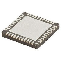
DS92LX2121SQE/NOPB National Semiconductor, DS92LX2121SQE/NOPB Datasheet - Page 9

DS92LX2121SQE/NOPB
Manufacturer Part Number
DS92LX2121SQE/NOPB
Description
IC SER/DESER 10-50MHZ 40-LLP
Manufacturer
National Semiconductor
Datasheet
1.DS92LX2121SQXNOPB.pdf
(38 pages)
Specifications of DS92LX2121SQE/NOPB
Serdes Function
Serializer
Data Rate
100Kbps
Ic Output Type
CML
No. Of Inputs
21
No. Of Outputs
2
Supply Voltage Range
3V To 3.6V
Driver Case Style
LLP
No. Of Pins
40
Msl
MSL 3 - 168 Hours
Rohs Compliant
Yes
Leaded Process Compatible
Yes
Lead Free Status / RoHS Status
Lead free / RoHS Compliant
Other names
DS92LX2121SQE/NOPBTR
I
I
CML DRIVER DC SPECIFICATIONS (DOUT+, DOUT-)
|V
ΔV
V
ΔV
I
R
CML RECEIVER DC SPECIFICATIONS (RIN+, RIN-)
V
V
V
I
R
SER/DES SUPPLY CURRENT *DIGITAL, PLL, AND ANALOG VDDS
I
I
I
I
OS
OZ
OS
IN
DDT
DDIOT
DDTZ
DDIOTZ
Symbol
OS
TH
TL
IN
T
T
OD
OD
OS
|
Output Short Circuit Current
TRI-STATE® Output Current RPWDNB = 0V,
Output Differential Voltage
Output Differential Voltage
Unbalance
Output Differential Offset
Voltage
Offset Voltage Unbalance
Output Short Circuit Current
Differential Internal
Termination Resistance
Differential Threshold High
Voltage
Differential Threshold Low
Voltage
Differential Input Voltage
Range
Input Current
Differential Internal
Termination Resistance
Serializer (Tx)
Total Supply Current Mode
(includes load current)
Serializer (Tx)
VDDIO Supply Current
(includes load current)
Serializer (Tx) Supply Current
Power-down
Parameter
V
V
R
R
R
RL = 100Ω
DOUT+/- = 0V,
PDB = L or H
Differential across DOUT+ and DOUT-
V
RIN+ - RIN-
V
V
Differential across RIN+ and RIN-
RT = 100Ω
WORST CASE pattern
(Figure
RT = 100Ω
RANDOM pattern
RT = 100Ω WORST CASE
pattern
PDB = 0V; All other
LVCMOS Inputs = 0V
OUT
OUT
CM
IN
DD
T
L
L
= 100Ω
= 100Ω
= 100Ω
= V
= 1.89 V
= 1.2V
= 0V
= 0V or V
DD
(Figure
4)
or 0 V,
(Note
(Figure
(Figure
(Note
DD
4)
Conditions
11)
6)
6)
11)
9
Serializer GPO
Outputs
Deserializer
LVCMOS
Outputs
Register
Address
(OSS_SEL = 0)
V
f = 50 MHz
Default
Registers
V
PCLK = 50 MHz
Default
Registers
V
PCLK = 50 MHz
Default
Registers
V
V
V
DDn
DDIO
DDIO
DD
DDIO
DDIO
= 1.89 V
= 1.89 V
= 1.89 V
= 3.6 V
= 1.89 V
= 3.6 V
V
V
DD (MIN)
OD (MAX)
Min
268
180
-20
-90
-20
80
80
-
V
DD
Typ
340
100
100
370
-11
-20
-27
±1
±1
62
55
55
65
1
1
2
7
- V
OD
V
V
DD (MAX)
OD (MIN)
Max
+20
412
120
+90
+20
120
775
125
135
50
50
90
15
5
www.national.com
-
Units
mA
mV
mV
mV
mA
mV
mV
mA
mA
µA
µA
µA
Ω
Ω
V


