VBP104FASR Vishay, VBP104FASR Datasheet
VBP104FASR
Specifications of VBP104FASR


Related parts for VBP104FASR

VBP104FASR Summary of contents
Page 1
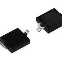
... DESCRIPTION VBP104FAS and VBP104FASR are high speed and high sensitive PIN photodiodes surface mount device (SMD) including the chip with a 4 daylight blocking filter matched with IR emitters operating at wavelength 870 nm or 950 nm. PRODUCT SUMMARY COMPONENT VBP104FAS VBP104FASR Note • Test conditions see table “Basic Characteristics” ...
Page 2
... VBP104FAS, VBP104FASR Vishay Semiconductors BASIC CHARACTERISTICS (T PARAMETER Forward voltage Breakdown voltage Reverse dark current Diode capacitance Open circuit voltage Temperature coefficient Short circuit current Temperature coefficient Reverse light current Angle of half sensitivity Wavelength of peak sensitivity Range of spectral bandwidth Noise equivalent power ...
Page 3
... V R λ = 950 21743 Fig Relative Spectral Sensitivity vs. Wavelength 100 94 8406 Fig Relative Radiant Sensitivity vs. Angular Displacement 100 detectortechsupport@vishay.com VBP104FAS, VBP104FASR Vishay Semiconductors 1.0 0.9 0.8 0.7 0.6 0.5 0.4 0.3 0.2 0.1 0.0 600 700 800 900 1000 λ - Wavelength (nm) 0° ...
Page 4
... VBP104FAS, VBP104FASR Vishay Semiconductors PACKAGE DIMENSIONS FOR VBP104FAS in millimeters Anode Cathode technical drawings according to DIN specifications Drawing-No.: 6.541-5088.01-4 Issue: 1; 15.04.10 22107 www.vishay.com For technical questions, contact: 4 Silicon PIN Photodiode Flat area 0.3 min. 4.4 ± 0.1 2.2 1 ± 0.15 6.4 ± 0.3 Recommended solder pad 8 ...
Page 5
... PACKAGE DIMENSIONS FOR VBP104FASR in millimeters Cathode Anode technical drawings according to DIN specifications Drawing-No.: 6.541-5087.01-4 Issue: 1; 15.04.10 22106 Document Number: 81169 For technical questions, contact: Rev. 1.1, 20-Apr-10 VBP104FAS, VBP104FASR Silicon PIN Photodiode Flat area 0.3 min. 4.4 ± 0.1 2.2 1 ± 0.15 6.4 ± ...
Page 6
... VBP104FAS, VBP104FASR Vishay Semiconductors TAPING DIMENSIONS FOR VBP104FAS in millimeters 21730 TAPING DIMENSIONS FOR VBP104FASR in millimeters 21731 www.vishay.com For technical questions, contact: 6 Silicon PIN Photodiode detectortechsupport@vishay.com Document Number: 81169 Rev. 1.1, 20-Apr-10 ...
Page 7
... REEL DIMENSIONS FOR VBP104FAS AND VBP104FASR in millimeters 21732 SOLDER PROFILE 300 255 °C 250 240 °C 217 °C 200 max 150 max. 100 s max. 120 s 100 50 max. ramp up 3 °C/s max. ramp down 6 °C 100 150 200 19841 Time (s) Fig Lead (Pb)-free Reflow Solder Profile acc ...
Page 8
... Vishay product could result in personal injury or death. Customers using or selling Vishay products not expressly indicated for use in such applications their own risk and agree to fully indemnify and hold Vishay and its distributors harmless from and against any and all claims, liabilities, expenses and damages arising or resulting in connection with such use or sale, including attorneys fees, even if such claim alleges that Vishay or its distributor was negligent regarding the design or manufacture of the part ...