TSL202R TAOS, TSL202R Datasheet - Page 2
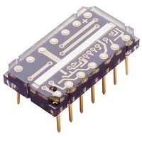
TSL202R
Manufacturer Part Number
TSL202R
Description
Photodiodes Linear Array 200 DPI
Manufacturer
TAOS
Type
Linear Sensor Arrayr
Datasheet
1.TSL202R.pdf
(12 pages)
Specifications of TSL202R
Peak Wavelength
1000 nm
Maximum Rise Time
500 ns
Maximum Fall Time
500 ns
Maximum Operating Temperature
+ 70 C
Minimum Operating Temperature
0 C
Product
Photodiode
Lead Free Status / RoHS Status
Lead free / RoHS Compliant
Available stocks
Company
Part Number
Manufacturer
Quantity
Price
Company:

Part Number:
TSL202R
Manufacturer:
TAOS
Quantity:
2 330


TSL202R
128 y 1 LINEAR SENSOR ARRAY
TAOS032C − MAY 2007
Terminal Functions
Detailed Description
2
Copyright E 2007, TAOS Inc.
†
The sensor consists of 128 photodiodes arranged in a linear array. Light energy impinging on a photodiode
generates photocurrent, which is integrated by the active integration circuitry associated with that pixel. During
the integration period, a sampling capacitor connects to the output of the integrator through an analog switch.
The amount of charge accumulated at each pixel is directly proportional to the light intensity and the integration
time. The integration time is the interval between two consecutive output periods.
The output and reset of the integrators is controlled by a 128-bit shift register and reset logic. An output cycle
is initiated by clocking in a logic 1 on SI for one positive going clock edge (see Figures1 and 2)
is clocked through the 128-bit shift register, the charge on the sampling capacitor of each pixel is sequentially
connected to a charge-coupled output amplifier that generates a voltage output, AO. When the bit position goes
low, the pixel integrator is reset. On the 129
and the output assumes a high-impedance state. Note that this 129
output of the 128
as early as the 130
The voltage developed at analog output (AO) is given by:
where:
AO is driven by a source follower that requires an external pulldown resistor (330-Ω typical). The output is
nominally 0 V for no light input, 2 V for normal white-level, and 3.4 V for saturation light level. When the device
is not in the output phase, AO is in a high impedance state.
A 0.1 μF bypass capacitor should be connected between V
For proper operation, after meeting the minimum hold time condition, SI must go low before the next rising edge of the clock.
AO1
AO2
CLK
GND
NC
SI1
SI2
SO1
SO2
V
NAME
DD
V
V
R
E
t
int
out
drk
e
e
TERMINAL
7, 9, 11, 14 No internal connection
is the analog output voltage for white condition
is the analog output voltage for dark condition
is the device responsivity for a given wavelength of light given in V/(μJ/cm
is the incident irradiance in μW/cm
is integration time in seconds
5,12
NO.
10
13
4
8
3
2
6
1
th
pixel and return the internal logic to a known state. A subsequent SI pulse can be presented
th
clock pulse, thereby initiating another pixel output cycle.
Analog output of section 1
Analog output of section 2
Clock. Clk controls charge transfer, pixel output, and reset.
Ground (substrate). All voltages are referenced to GND.
Serial input (section 1). SI1 defines the start of the data-out sequence.
Serial input (section 2). SI2 defines the start of the data-out sequence.
Serial output (section 1). SO1 provides a signal to drive the SI2 input.
Serial output (section 2). SO2 provides a signal to drive the SI input of another device for
cascading or as an end-of-data indication.
Supply voltage. Supply voltage for both analog and digital circuitry.
V
out
= V
r
drk
+ (R
www.taosinc.com
th
e
2
clock rising edge, the SI pulse is clocked out of the shift register
) (E
e
) (t
int
)
DESCRIPTION
DD
and ground as close as possible to the device.
th
clock pulse is required to terminate the
r
2
The LUMENOLOGY r Company
)
†
. As the SI pulse
Related parts for TSL202R
Image
Part Number
Description
Manufacturer
Datasheet
Request
R

Part Number:
Description:
Microcontroller Modules & Accessories TAOS Eval Module w/USB Interface
Manufacturer:
TAOS
Part Number:
Description:
Optical Sensor Development Tools TAOS Eval Module
Manufacturer:
TAOS

Part Number:
Description:
Industrial Optical Sensors Ambient Light Sensor SMBus
Manufacturer:
TAOS
Datasheet:

Part Number:
Description:
Photodiodes TriColor Sensor RGB, Clear Ch
Manufacturer:
TAOS
Datasheet:

Part Number:
Description:
LED Displays Hexadecimal Display 4-bit
Manufacturer:
TAOS
Datasheet:

Part Number:
Description:
Photodiodes Linear Sensor Array 200dpi 64pix
Manufacturer:
TAOS
Datasheet:

Part Number:
Description:
Industrial Optical Sensors Ambient Light Sensor SMBus
Manufacturer:
TAOS
Datasheet:

Part Number:
Description:
Photodiodes Linear Array 200 DPI
Manufacturer:
TAOS
Datasheet:

Part Number:
Description:
Photodiodes Light to Voltage Converter
Manufacturer:
TAOS
Datasheet:

Part Number:
Description:
Photodiodes Linear Array 200 DPI
Manufacturer:
TAOS
Datasheet:
Part Number:
Description:
Industrial Optical Sensors Ambient Light Sensor SMBus
Manufacturer:
TAOS
Datasheet:
Part Number:
Description:
Photodiodes TriColor Sensor RGB, Clear Ch
Manufacturer:
TAOS
Datasheet:
Part Number:
Description:
LED Displays Hexadecimal Display 4-bit
Manufacturer:
TAOS
Datasheet:
Part Number:
Description:
Photodiodes Linear Sensor Array 200dpi 64pix
Manufacturer:
TAOS
Datasheet:
